Datasheet 搜索 > 逻辑控制器 > TI(德州仪器) > SN74LVC125AMDREP 数据手册 > SN74LVC125AMDREP 数据手册 1/14 页
 器件3D模型
¥ 6.717
SN74LVC125AMDREP 数据手册 - TI(德州仪器)
制造商:
TI(德州仪器)
分类:
逻辑控制器
封装:
SOIC-14
描述:
具有三态输出的增强型产品四路总线缓冲门 14-SOIC -55 to 125
Pictures:
3D模型
符号图
焊盘图
引脚图
产品图
页面导航:
导航目录
SN74LVC125AMDREP数据手册
Page:
of 14 Go
若手册格式错乱,请下载阅览PDF原文件
www.ti.com
FEATURES
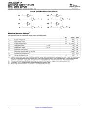
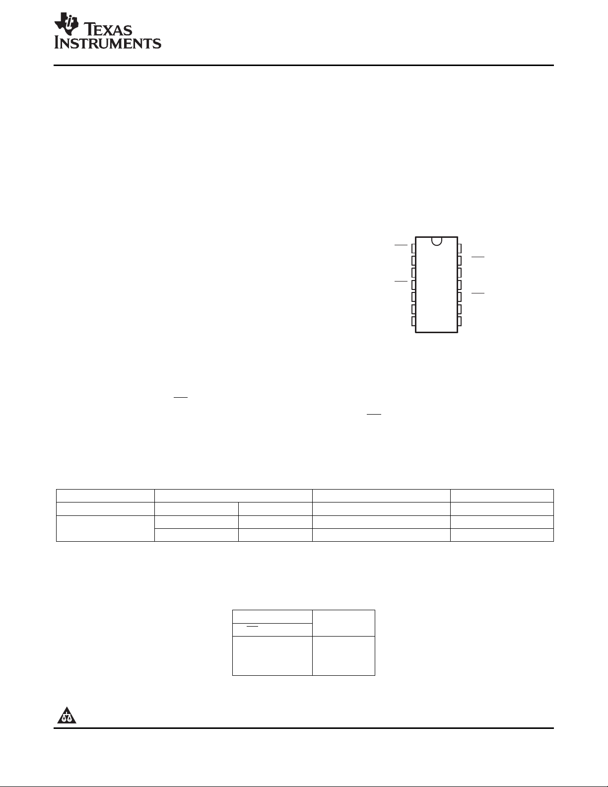
PW PACKAGE
(TOP VIEW)
1
2
3
4
5
6
7
14
13
12
11
10
9
8
1OE
1A
1Y
2OE
2A
2Y
GND
V
CC
4OE
4A
4Y
3OE
3A
3Y
DESCRIPTION/ORDERING INFORMATION
SN74LVC125A-EP
QUADRUPLE BUS BUFFER GATE
WITH 3-STATE OUTPUTS
SCAS739C – DECEMBER 2003 – REVISED DECEMBER 2006
• Controlled Baseline • Typical V
OHV
(Output V
OH
Undershoot) >2 V at
V
CC
= 3.3 V, T
A
= 25 ° C
– One Assembly/Test Site, One Fabrication
Site • Latch-Up Performance Exceeds 250 mA Per
JESD 17
• Enhanced Diminishing Manufacturing Sources
(DMS) Support • ESD Protection Exceeds JESD 22
• Enhanced Product-Change Notification – 2000-V Human-Body Model (A114-A)
• Qualification Pedigree
(1)
– 200-V Machine Model (A115-A)
• Operates From 1.65 V to 3.6 V – 1000-V Charged-Device Model (C101)
• Inputs Accept Voltages to 5.5 V
• Max t
pd
of 4.8 ns at 3.3 V
• Typical V
OLP
(Output Ground Bounce) <0.8 V
at V
CC
= 3.3 V, T
A
= 25 ° C
(1) Component qualification in accordance with JEDEC and
industry standards to ensure reliable operation over an
extended temperature range. This includes, but is not limited
to, Highly Accelerated Stress Test (HAST) or biased 85/85,
temperature cycle, autoclave or unbiased HAST,
electromigration, bond intermetallic life, and mold compound
life. Such qualification testing should not be viewed as
justifying use of this component beyond specified
performance and environmental limits.
This quadruple bus buffer gate is designed for 1.65-V to 3.6-V V
CC
operation.
The SN74LVC125A features independent line drivers with 3-state outputs. Each output is disabled when the
associated output-enable ( OE) input is high.
To ensure the high-impedance state during power up or power down, OE should be tied to V
CC
through a pullup
resistor; the minimum value of the resistor is determined by the current-sinking capability of the driver.
Inputs can be driven from either 3.3-V or 5-V devices. This feature allows the use of this device as a translator in
a mixed 3.3-V/5-V system environment.
ORDERING INFORMATION
T
A
PACKAGE
(1)
ORDERABLE PART NUMBER TOP-SIDE MARKING
–40 ° C to 85 ° C TSSOP – PW Reel of 2000 SN74LVC125AIPWREP C125AEP
TSSOP – PW Reel of 2000 SN74LVC125AMPWREP
(2)
125AMEP
–55 ° C to 125 ° C
SOIC – D Reel of 2500 SN74LVC125AMDREP 125AMEP
(1) Package drawings, standard packing quantities, thermal data, symbolization, and PCB design guidelines are available at
www.ti.com/sc/package.
(2) Product Preview
FUNCTION TABLE
(EACH BUFFER)
INPUTS
OUTPUT
Y
OE A
L H H
L L L
H X Z
Please be aware that an important notice concerning availability, standard warranty, and use in critical applications of Texas
Instruments semiconductor products and disclaimers thereto appears at the end of this data sheet.
PRODUCTION DATA information is current as of publication date.
Copyright © 2003–2006, Texas Instruments Incorporated
Products conform to specifications per the terms of the Texas
Instruments standard warranty. Production processing does not
necessarily include testing of all parameters.
器件 Datasheet 文档搜索
AiEMA 数据库涵盖高达 72,405,303 个元件的数据手册,每天更新 5,000 多个 PDF 文件
