Datasheet 搜索 > 逻辑芯片 > TI(德州仪器) > SN74LVC125APWRG3 数据手册 > SN74LVC125APWRG3 数据手册 1/28 页

 器件3D模型
¥ 1.191
SN74LVC125APWRG3 数据手册 - TI(德州仪器)
制造商:
TI(德州仪器)
分类:
逻辑芯片
封装:
TSSOP-14
描述:
缓冲器和线路驱动器 Quad Bus Buffer Gate
Pictures:
3D模型
符号图
焊盘图
引脚图
产品图
页面导航:
引脚图在P3Hot
典型应用电路图在P10P11
原理图在P1P9P10
封装尺寸在P14P15P17P18
标记信息在P14P15P16
封装信息在P13P14P15P16P17P18
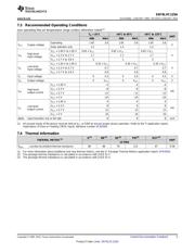
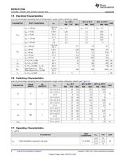
技术参数、封装参数在P4P10
应用领域在P1P16P28
电气规格在P6
型号编号列表在P10
导航目录
SN74LVC125APWRG3数据手册
Page:
of 28 Go
若手册格式错乱,请下载阅览PDF原文件
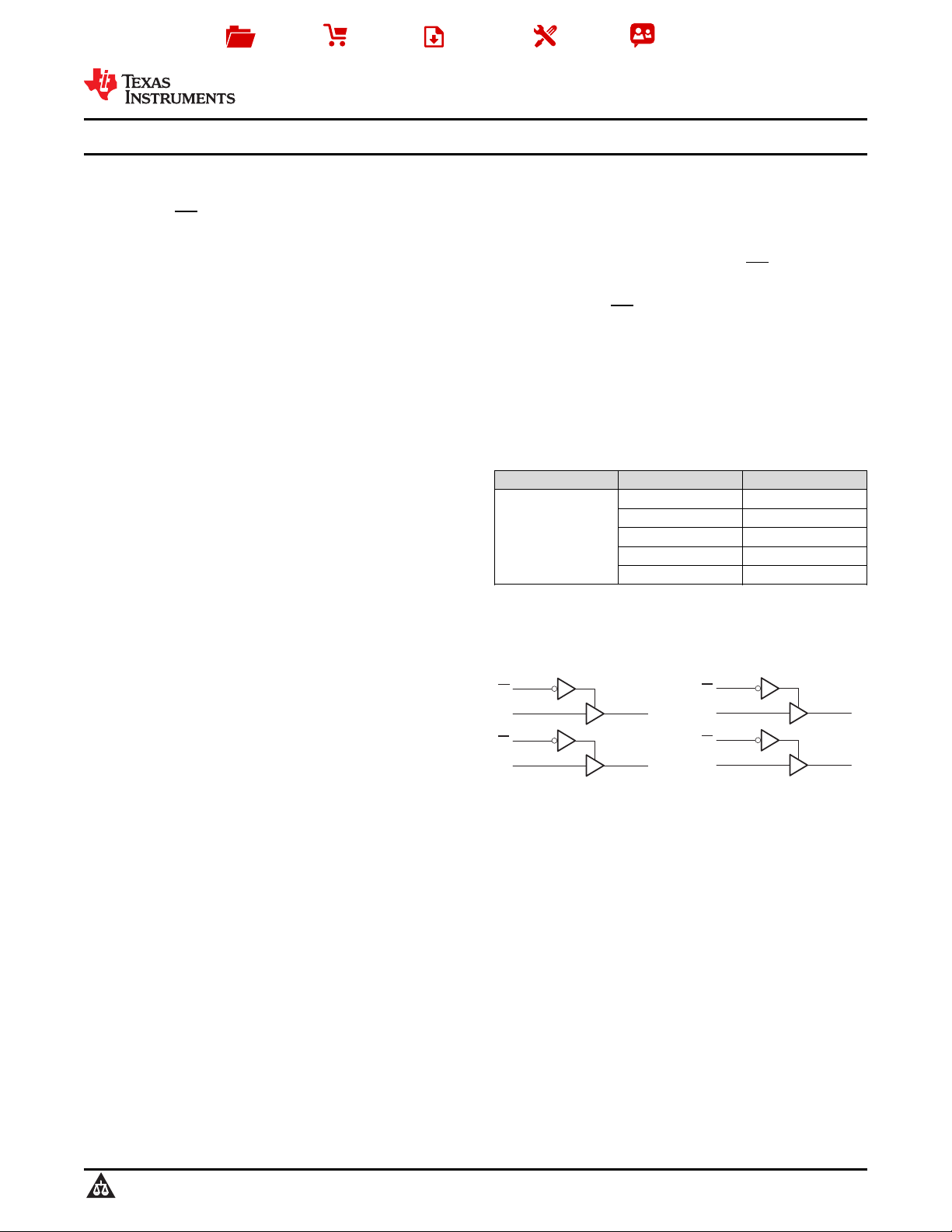
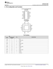
2A 2Y
2OE
1A 1Y
1OE
4A 4Y
4OE
3A 3Y
3OE
Product
Folder
Sample &
Buy
Technical
Documents
Tools &
Software
Support &
Community
SN74LVC125A
SCAS290Q –JANUARY 1993–REVISED JANUARY 2015
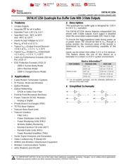
SN74LVC125A Quadruple Bus Buffer Gate With 3-State Outputs
1 Features 3 Description
This quadruple bus buffer gate is designed for 1.65-V
1
• 3-State Outputs
to 3.6-V V
CC
operation.
• Separate OE for all 4 buffers
The SN74LVC125A device features independent line
• Operates From 1.65 V to 3.6 V
drivers with 3-state outputs. Each output is disabled
• Specified From –40°C to 85°C
when the associated output-enable (OE) input is high.
and –40°C to 125°C
To ensure the high-impedance state during power up
• Inputs Accept Voltages to 5.5 V
or power down, OE should be tied to V
CC
through a
• Max t
pd
of 4.8 ns at 3.3 V
pullup resistor; the minimum value of the resistor is
determined by the current-sinking capability of the
• Typical V
OLP
(Output Ground Bounce)
driver.
< 0.8 V at V
CC
= 3.3 V, T
A
= 25°C
• Typical V
OHV
(Output V
OH
Undershoot)
Inputs can be driven from either 3.3-V or 5-V devices.
> 2 V at V
CC
= 3.3 V, T
A
= 25°C
This feature allows the use of this device as a
translator in a mixed 3.3-V/5-V system environment.
• Latch-Up Performance Exceeds 250 mA
Per JESD 17
Device Information
(1)
• ESD Protection Exceeds JESD 22
PART NUMBER PACKAGE (PIN) BODY SIZE
– 2000-V Human-Body Model
SOIC (14) 8.65 mm × 3.91 mm
– 200-V Machine Model
SSOP (14) 6.20 mm × 5.30 mm
SN74LVC125A SOP (14) 10.30 mm × 5.30 mm
– 1000-V Charged-Device Model
TSSOP (14) 5.00 mm × 4.40 mm
VQFN (14) 3.50 mm × 3.50 mm
2 Applications
(1) For all available packages, see the orderable addendum at
• Cable Modem Termination Systems
the end of the data sheet.
• IP Phones: Wired and Wireless
• Optical Modules
4 Simplified Schematic
• Optical Networking:
– EPON or Video Over Fiber
• Point-to-Point Microwave Backhaul
• Power: Telecom DC/DC Modules:
– Analog or Digital
• Private Branch Exchanges (PBX)
• TETRA Base Stations
• Telecom Base Band Units
• Telecom Shelters:
– Filter Unit s
– Power Distribution Units (PDU)
– Power Monitoring Units (PMU)
– Wireless Battery Monitoring
– Remote Electrical Tilt Units (RET)
– Remote Radio Units (RRU)
– Tower Mounted Amplifiers (TMA)
• Vector Signal Analyzers and Generators
• Video Conferencing: IP-Based HD
• WiMAX and Wireless Infrastructure Equipment
• Wireless Communications Testers
• xDSL Modems and DSLAM
1
An IMPORTANT NOTICE at the end of this data sheet addresses availability, warranty, changes, use in safety-critical applications,
intellectual property matters and other important disclaimers. PRODUCTION DATA.
器件 Datasheet 文档搜索
AiEMA 数据库涵盖高达 72,405,303 个元件的数据手册,每天更新 5,000 多个 PDF 文件
