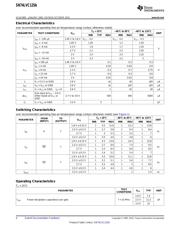
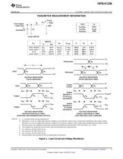
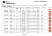
Datasheet 搜索 > 逻辑控制器 > TI(德州仪器) > SN74LVC125APWR 数据手册 > SN74LVC125APWR 数据手册 1/20 页
 器件3D模型
¥ 0.421
SN74LVC125APWR 数据手册 - TI(德州仪器)
制造商:
TI(德州仪器)
分类:
逻辑控制器
封装:
TSSOP-14
描述:
TEXAS INSTRUMENTS SN74LVC125APWR 缓冲器/线路驱动器, 非反相, 3态, 4门, 1输入, 1.65V至3.6V, TSSOP-14
Pictures:
3D模型
符号图
焊盘图
引脚图
产品图
页面导航:
导航目录
SN74LVC125APWR数据手册
Page:
of 20 Go
若手册格式错乱,请下载阅览PDF原文件
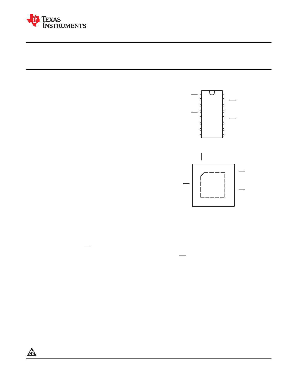
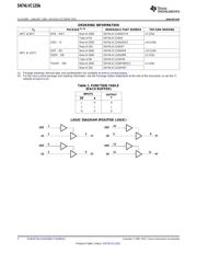
D, DB, NS, OR PW PACKAGE
(TOP VIEW)
1
2
3
4
5
6
7
14
13
12
11
10
9
8
1OE
1A
1Y
2OE
2A
2Y
GND
V
CC
4OE
4A
4Y
3OE
3A
3Y
RGY PACKAGE
(TOP VIEW)
1 14
7 8
2
3
4
5
6
13
12
11
10
9
4OE
4A
4Y
3OE
3A
1A
1Y
2OE
2A
2Y
1OE
3Y
V
GND
CC
SN74LVC125A
www.ti.com
SCAS290P –JANUARY 1993–REVISED OCTOBER 2010
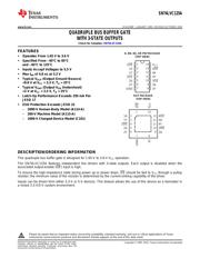
QUADRUPLE BUS BUFFER GATE
WITH 3-STATE OUTPUTS
Check for Samples: SN74LVC125A
1
FEATURES
• Operates From 1.65 V to 3.6 V
• Specified From –40°C to 85°C
and –40°C to 125°C
• Inputs Accept Voltages to 5.5 V
• Max t
pd
of 4.8 ns at 3.3 V
• Typical V
OLP
(Output Ground Bounce)
<0.8 V at V
CC
= 3.3 V, T
A
= 25°C
• Typical V
OHV
(Output V
OH
Undershoot)
>2 V at V
CC
= 3.3 V, T
A
= 25°C
• Latch-Up Performance Exceeds 250 mA Per
JESD 17
• ESD Protection Exceeds JESD 22
– 2000-V Human-Body Model (A114-A)
– 200-V Machine Model (A115-A)
– 1000-V Charged-Device Model (C101)
DESCRIPTION/ORDERING INFORMATION
This quadruple bus buffer gate is designed for 1.65-V to 3.6-V V
CC
operation.
The SN74LVC125A features independent line drivers with 3-state outputs. Each output is disabled when the
associated output-enable (OE) input is high.
To ensure the high-impedance state during power up or power down, OE should be tied to V
CC
through a pullup
resistor; the minimum value of the resistor is determined by the current-sinking capability of the driver.
Inputs can be driven from either 3.3-V or 5-V devices. This feature allows the use of this device as a translator in
a mixed 3.3-V/5-V system environment.
1
Please be aware that an important notice concerning availability, standard warranty, and use in critical applications of Texas
Instruments semiconductor products and disclaimers thereto appears at the end of this data sheet.
PRODUCTION DATA information is current as of publication date.
Copyright © 1993–2010, Texas Instruments Incorporated
Products conform to specifications per the terms of the Texas
Instruments standard warranty. Production processing does not
necessarily include testing of all parameters.
器件 Datasheet 文档搜索
AiEMA 数据库涵盖高达 72,405,303 个元件的数据手册,每天更新 5,000 多个 PDF 文件
