Datasheet 搜索 > 逻辑控制器 > TI(德州仪器) > SN74LVC244ADBR 数据手册 > SN74LVC244ADBR 数据手册 4/31 页
 器件3D模型
¥ 0.738
SN74LVC244ADBR 数据手册 - TI(德州仪器)
制造商:
TI(德州仪器)
分类:
逻辑控制器
封装:
SSOP-20
描述:
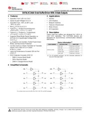
74LVC 系列反相器和缓冲器,德州仪器德州仪器的 74LVC 系列低功率 CMOS 逻辑集 IC 的一系列反相器和缓冲器。 74LVC 系列使用硅门 CMOS 技术,设计用于在 3.3V 时工作,与 5V 系统相比,允许功耗显著降低。工作电压:1.65 至 3.6V 5V 容差的输入 兼容性:输入 LVTTL/TTL,输出 LVCMOS 按 JESD 17标准,闩锁效应性能超过 250 mA ESD 保护超过 JESD 22 ### 74LVC 系列
Pictures:
3D模型
符号图
焊盘图
引脚图
产品图
页面导航:
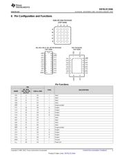
引脚图在P3Hot
典型应用电路图在P10P11
原理图在P1P9P10
封装尺寸在P13P14P16P17
标记信息在P13P14P15
封装信息在P12P13P14P15P16P17
技术参数、封装参数在P4P10
应用领域在P1P31
电气规格在P6
型号编号列表在P10
导航目录
SN74LVC244ADBR数据手册
Page:
of 31 Go
若手册格式错乱,请下载阅览PDF原文件
SN74LVC244A
SCAS414Z –NOVEMBER 1992–REVISED JANUARY 2015
www.ti.com
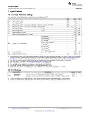
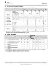
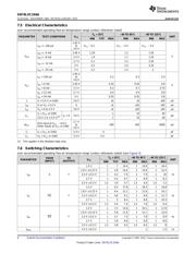
7 Specifications
7.1 Absolute Maximum Ratings
over operating free-air temperature range (unless otherwise noted)
(1)
MIN MAX UNIT
V
CC
Supply voltage range –0.5 6.5 V
V
I
Input voltage range
(2)
–0.5 6.5 V
V
O
Voltage range applied to any output in the high-impedance or power-off state
(2)
–0.5 6.5 V
V
O
Voltage range applied to any output in the high or low state
(2)(3)
–0.5 V
CC
+ 0.5 V
I
IK
Input clamp current V
I
< 0 –50 mA
I
OK
Output clamp current V
O
< 0 –50 mA
I
O
Continuous output current ±50 mA
Continuous current through V
CC
or GND ±100 mA
DB package
(4)
70
DGV package
(4)
92
DW package
(4)
58
GQN or ZQN package
(4)
78
θ
JA
Package thermal impedance °C/W
N package
(4)
69
NS package
(4)
60
PW package
(4)
83
RGY package
(5)
37
P
tot
Power dissipation T
A
= –40°C to 125°C
(6)(7)
500 mW
T
stg
Storage temperature range –65 150 °C
(1) Stresses beyond those listed under Absolute Maximum Ratings may cause permanent damage to the device. These are stress ratings
only, and functional operation of the device at these or any other conditions beyond those indicated under Recommended Operating
Conditions is not implied. Exposure to absolute-maximum-rated conditions for extended periods may affect device reliability.
(2) The input and output negative-voltage ratings may be exceeded if the input and output current ratings are observed.
(3) The value of V
CC
is provided in the Recommended Operating Conditions table.
(4) The package thermal impedance is calculated in accordance with JESD 51-7.
(5) The package thermal impedance is calculated in accordance with JESD 51-5.
(6) For the DW package: above 70°C the value of P
tot
derates linearly with 8 mW/K.
(7) For the DB, DGV, N, NS, and PW packages: above 60°C the value of P
tot
derates linearly with 5.5 mW/K.
7.2 ESD Ratings
PARAMETER DEFINITION VALUE UNIT
Human body model (HBM), per ANSI/ESDA/JEDEC JS-001, all pins
(1)
2000
Electrostatic
V
(ESD)
V
discharge
Charged device model (CDM), per JEDEC specification JESD22-C101, all pins
(2)
1000
(1) JEDEC document JEP155 states that 500-V HBM allows safe manufacturing with a standard ESD control process.
(2) JEDEC document JEP157 states that 250-V CDM allows safe manufacturing with a standard ESD control process.
4 Submit Documentation Feedback Copyright © 1992–2015, Texas Instruments Incorporated
Product Folder Links: SN74LVC244A
器件 Datasheet 文档搜索
AiEMA 数据库涵盖高达 72,405,303 个元件的数据手册,每天更新 5,000 多个 PDF 文件
