Datasheet 搜索 > 逻辑控制器 > TI(德州仪器) > SN74LVC244APW 数据手册 > SN74LVC244APW 数据手册 9/33 页
 器件3D模型
¥ 3.813
SN74LVC244APW 数据手册 - TI(德州仪器)
制造商:
TI(德州仪器)
分类:
逻辑控制器
封装:
TSSOP-20
描述:
八路缓冲器/驱动器,具有三态输出 OCTAL BUFFER/DRIVER WITH 3-STATE OUTPUTS
Pictures:
3D模型
符号图
焊盘图
引脚图
产品图
页面导航:
引脚图在P3P4Hot
典型应用电路图在P1P9P10P11
原理图在P9P10
封装尺寸在P13P14P16P17P25P29
焊盘布局在P26P30
标记信息在P13P14P15
封装信息在P12P13P14P15P16P17
技术参数、封装参数在P4P10
应用领域在P1
电气规格在P6
型号编号列表在P10
导航目录
SN74LVC244APW数据手册
Page:
of 33 Go
若手册格式错乱,请下载阅览PDF原文件
1
2 18
1Y1
1OE
1A1
4 16
1Y2
1A2
6 14
1Y3
1A3
8 12
1Y4
1A4
19
11 9
2Y1
2OE
2A1
13 7
2Y2
2A2
15 5
2Y3
2A3
17 3
2Y4
2A4
Pin numbers shown are for the DB, DGV, DW, N, NS, PW, and RGY packages.
9
SN74LVC244A
www.ti.com
SCAS414AB –NOVEMBER 1992–REVISED NOVEMBER 2016
Product Folder Links: SN74LVC244A
Submit Documentation FeedbackCopyright © 1992–2016, Texas Instruments Incorporated
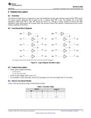
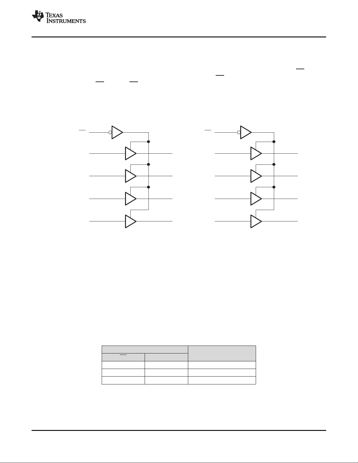
8 Detailed Description
8.1 Overview
The SN74LVC244A device is organized as two 4-bit buffers/line drivers with separate output-enable (OE) inputs.
The device passes data from the A inputs to the Y outputs when OE is low. The outputs are in the high-
impedance state when OE is high. OE should be tied to V
CC
through a pullup resistor to ensure the high-
impedance state during power up or power down; the minimum value of the resistor is determined by the current-
sinking capability of the driver.
8.2 Functional Block Diagram
Figure 4. Logic Diagram (Positive Logic)
8.3 Feature Description
• Allows down voltage translation
– 5 V to 3.3 V
– 5 V or 3.3 V to 1.8 V
• Inputs accept voltage levels up to 5.5 V
• It is available in ultra small logic 20 pin QFN package at 0.5 mm max height with 0.4 mm pitch.
8.4 Device Functional Modes
Table 1 lists the functional modes of the SN74LVC244A.
Table 1. Function Table
INPUTS
OUTPUT
Y
OE A
L H H
L L L
H X Hi-Z
器件 Datasheet 文档搜索
AiEMA 数据库涵盖高达 72,405,303 个元件的数据手册,每天更新 5,000 多个 PDF 文件
