Datasheet 搜索 > MOS管 > Toshiba(东芝) > SSM3J14T(TE85L,F) 数据手册 > SSM3J14T(TE85L,F) 数据手册 1/6 页

¥ 3.313
SSM3J14T(TE85L,F) 数据手册 - Toshiba(东芝)
制造商:
Toshiba(东芝)
分类:
MOS管
封装:
TSM
Pictures:
3D模型
符号图
焊盘图
引脚图
产品图
页面导航:
标记信息在P1
技术参数、封装参数在P1
应用领域在P6
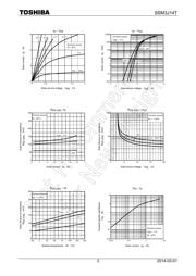
电气规格在P2
导航目录
SSM3J14T(TE85L,F)数据手册
Page:
of 6 Go
若手册格式错乱,请下载阅览PDF原文件
SSM3J14T
2014-03-01
1
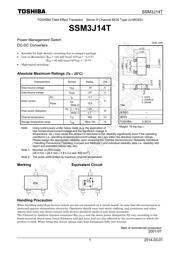
TOSHIBA Field Effect Transistor Silicon P Channel MOS Type (U-MOSII)
SSM3J14T
Power Management Switch
DC-DC Converters
• Suitable for high-density mounting due to compact package
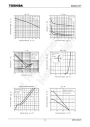
• Low on Resistance : R
on
= 145 mΩ (max) (@V
GS
= −4.5 V)
: R
on
= 85 mΩ (max) (@V
GS
= −10 V)
• High-speed switching
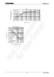
Absolute Maximum Ratings
(Ta
=
25°C)
Characteristics Symbol Rating Unit
Drain-Source voltage V
DS
−30
V
Gate-Source voltage V
GSS
±20
V
DC I
D
−2.7
Drain current
Pulse
I
DP
(Note 2)
−5.4
A
P
D
t = 10 s 1.25
Drain power dissipation
(Note 1) 0.7
W
Channel temperature T
ch
150 °C
Storage temperature range T
stg
−55 to 150 °C
Note: Using continuously under heavy loads (e.g. the application of
high temperature/current/voltage and the significant change in
temperature, etc.) may cause this product to decrease in the reliability significantly even if the operating
conditions (i.e. operating temperature/current/voltage, etc.) are within the absolute maximum ratings.
Please design the appropriate reliability upon reviewing the Toshiba Semiconductor Reliability Handbook
(“Handling Precautions”/“Derating Concept and Methods”) and individual reliability data (i.e. reliability test
report and estimated failure rate, etc).
Note 1: Mounted on FR4 board
(25.4 mm × 25.4 mm × 1.6 t, Cu pad: 645 mm
2
)
Note 2: The pulse width limited by maximum channel temperature.
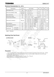
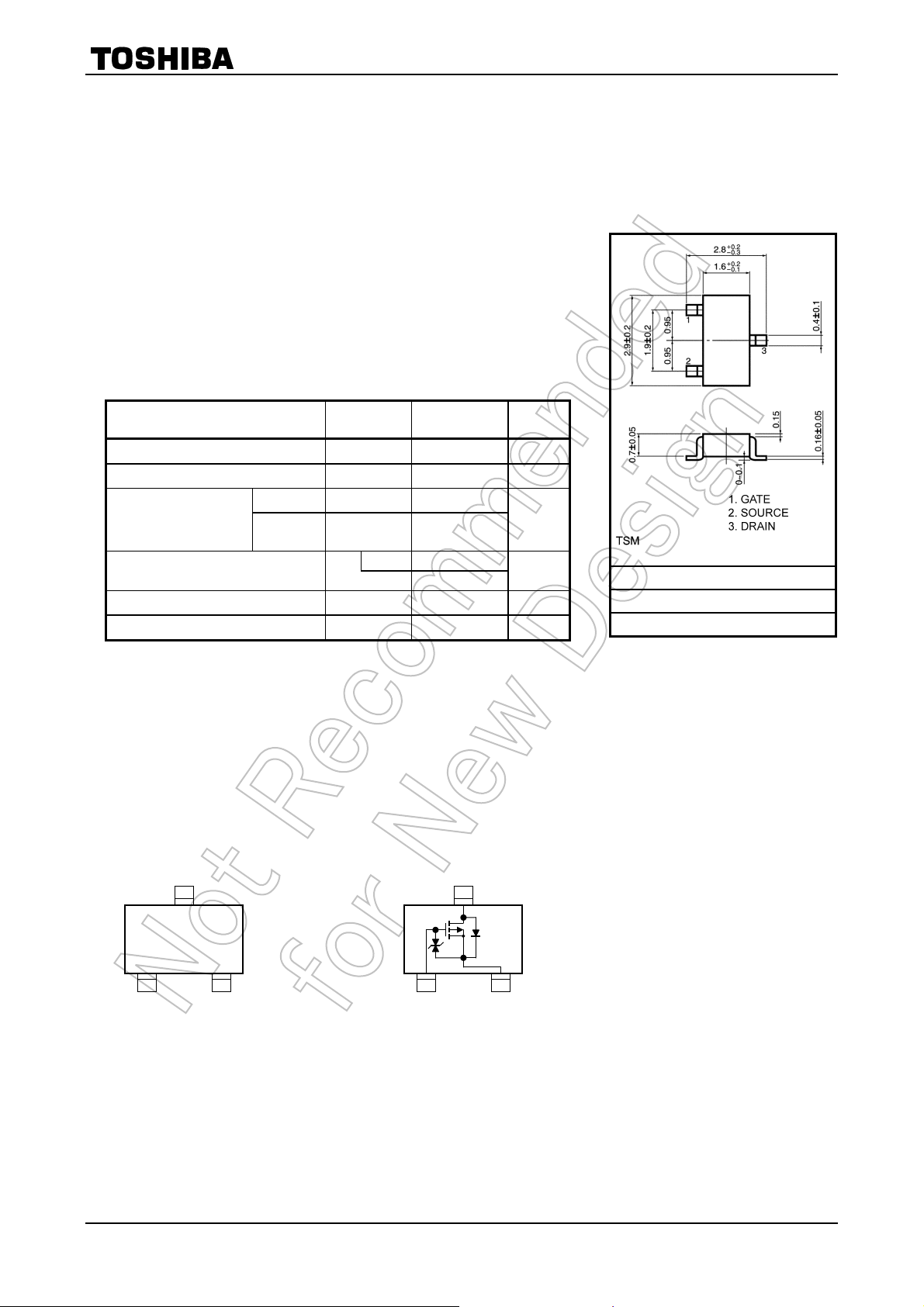
Marking Equivalent Circuit
Handling Precaution
When handling individual devices (which are not yet mounted on a circuit board), be sure that the environment is
protected against electrostatic electricity. Operators should wear anti-static clothing, and containers and other
objects that come into direct contact with devices should be made of anti-static materials.
The Channel-to-Ambient thermal resistance R
th (ch-a)
and the drain power dissipation P
D
vary according to the
board material, board area, board thickness and pad area, and are also affected by the environment in which the
product is used. When using this device, please take heat dissipation fully into account
Unit: mm
JEDEC ―
JEITA ―
TOSHIBA 2-3S1A
Weight: 10 mg (typ.)
3
1 2
KDL
3
12
Start of commercial production
2001-07
器件 Datasheet 文档搜索
AiEMA 数据库涵盖高达 72,405,303 个元件的数据手册,每天更新 5,000 多个 PDF 文件
