Datasheet 搜索 > Microchip(微芯) > SST25VF016B-50-4I-S2AE 数据手册 > SST25VF016B-50-4I-S2AE 数据手册 6/30 页


¥ 0
SST25VF016B-50-4I-S2AE 数据手册 - Microchip(微芯)
制造商:
Microchip(微芯)
Pictures:
3D模型
符号图
焊盘图
引脚图
产品图
页面导航:
引脚图在P4Hot
原理图在P3
封装信息在P24P25P28
技术参数、封装参数在P22
导航目录
SST25VF016B-50-4I-S2AE数据手册
Page:
of 30 Go
若手册格式错乱,请下载阅览PDF原文件
SST25VF016B
DS20005044C-page 6 2015 Microchip Technology Inc.
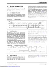
4.2.1 WRITE PROTECT PIN (WP#)
The Write Protect (WP#) pin enables the lock-down
function of the BPL bit (bit 7) in the status register.
When WP# is driven low, the execution of the Write-
Status-Register (WRSR) instruction is determined by
the value of the BPL bit (see
Table 4-1). When WP# is
high, the lock-down function of the BPL bit is disabled.
4.3 Status Register
The software status register provides status on
whether the flash memory array is available for any
Read or Write operation, whether the device is Write
enabled, and the state of the Memory Write protection.
During an internal Erase or Program operation, the sta-
tus register may be read only to determine the comple-
tion of an operation in progress.
Table 4-2 describes
the function of each bit in the software status register.
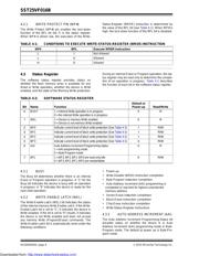
4.3.1 BUSY
The Busy bit determines whether there is an internal
Erase or Program operation in progress. A “1” for the
Busy bit indicates the device is busy with an operation
in progress. A “0” indicates the device is ready for the
next valid operation.
4.3.2 WRITE ENABLE LATCH (WEL)
The Write-Enable-Latch (WEL) bit indicates the status
of the internal memory Write Enable Latch. If the Write-
Enable-Latch bit is set to “1”, it indicates the device is
Write enabled. If the bit is set to “0” (reset), it indicates
the device is not Write enabled and does not accept
any memory Write (Program/Erase) commands. The
Write-Enable-Latch bit is automatically reset under the
following conditions:
• Power-up
• Write-Disable (WRDI) instruction completion
• Byte-Program instruction completion
• Auto Address Increment (AAI) programming is
completed or reached its highest unprotected
memory address
• Sector-Erase instruction completion
• Block-Erase instruction completion
• Chip-Erase instruction completion
• Write-Status-Register instructions
4.3.3 AUTO ADDRESS INCREMENT (AAI)
The Auto Address Increment Programming-Status bit
provides status on whether the device is in Auto
Address Increment (AAI) programming mode or Byte-
Program mode. The default at power up is Byte-Pro-
gram mode.
TABLE 4-1: CONDITIONS TO EXECUTE WRITE-STATUS-REGISTER (WRSR) INSTRUCTION
WP# BPL Execute WRSR Instruction
L1Not Allowed
L0Allowed
HXAllowed
TABLE 4-2: SOFTWARE STATUS REGISTER
Bit Name Function
Default at
Power-up Read/Write
0 BUSY 1 = Internal Write operation is in progress
0 = No internal Write operation is in progress
0R
1 WEL 1 = Device is memory Write enabled
0 = Device is not memory Write enabled
0R
2 BP0 Indicate current level of block write protection (See
Table 4-3) 1R/W
3 BP1 Indicate current level of block write protection (See
Table 4-3) 1R/W
4 BP2 Indicate current level of block write protection (See
Table 4-3) 1R/W
5 BP3 Indicate current level of block write protection (See
Table 4-3) 0R/W
6 AAI Auto Address Increment Programming status
1 = AAI programming mode
0 = Byte-Program mode
0R
7 BPL 1 = BP3, BP2, BP1, BP0 are read-only bits
0 = BP3, BP2, BP1, BP0 are read/writable
0R/W
Downloaded from: http://www.datasheetcatalog.com/
器件 Datasheet 文档搜索
AiEMA 数据库涵盖高达 72,405,303 个元件的数据手册,每天更新 5,000 多个 PDF 文件
