Datasheet 搜索 > 接口芯片 > TI(德州仪器) > TFP401PZP 数据手册 > TFP401PZP 数据手册 4/32 页
 器件3D模型
¥ 36.957
TFP401PZP 数据手册 - TI(德州仪器)
制造商:
TI(德州仪器)
分类:
接口芯片
封装:
TQFP-100
描述:
TEXAS INSTRUMENTS TFP401PZP 专用接口, DVI, 台式LCD监控器, 数字式投影仪, 3 V, 3.6 V, HTQFP, 100 引脚
Pictures:
3D模型
符号图
焊盘图
引脚图
产品图
页面导航:
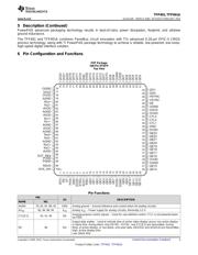
引脚图在P3P4P5Hot
典型应用电路图在P17
原理图在P12
封装尺寸在P27
标记信息在P27
封装信息在P1P25P27P28
技术参数、封装参数在P6
应用领域在P1P17P28P32
电气规格在P7P8P15
导航目录
TFP401PZP数据手册
Page:
of 32 Go
若手册格式错乱,请下载阅览PDF原文件
TFP401
,
TFP401A
SLDS120F –MARCH 2000–REVISED FEBRUARY 2015
www.ti.com
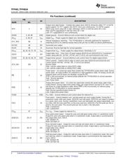
Pin Functions (continued)
PIN
I/O DESCRIPTION
NAME NO.
Output clock data format – Controls the output clock (ODCK) format for either TFT or DSTN
panel support. For TFT support, the ODCK clock runs continuously. For DSTN support,
DFO 1 DI ODCK only clocks when DE is high; otherwise, ODCK is held low when DE is low.
High: DSTN support/ODCK held low when DE = low
Low: TFT support/ODCK runs continuously.
DGND 5, 39, 68 GND Digital ground – Ground reference and current return for digital core
DV
DD
6, 38, 67 V
DD
Digital V
DD
– Power supply for digital core. Nominally 3.3 V
Internal impedance matching – The TFP401/401A is internally optimized for impedance
EXT_RES 96 AI
matching at 50 Ω. An external resistor tied to this pin has no effect on device performance.
HSYNC 48 DO Horizontal sync output
RSVD 99 DI Reserved. Must be tied high for normal operation
OV
DD
18, 29, 43, 57, 78 V
DD
Output driver V
DD
– Power supply for output drivers. Nominally 3.3 V
Output data clock – Pixel clock. All pixel outputs QE[23:0] and QO[23:0] (if in 2-pixel/clock
ODCK 44 DO
mode), along with DE, HSYNC, VSYNC and CTL[3:1], are synchronized to this clock.
OGND 19, 28, 45, 58, 76 GND Output driver ground – Ground reference and current return for digital output drivers
ODCK polarity – Selects ODCK edge on which pixel data (QE[23:0] and QO[23:0]) and
control signals (HSYNC, VSYNC, DE, CTL[3:1]) are latched.
OCK_INV 100 DI Normal mode:
High: Latches output data on rising ODCK edge
Low: Latches output data on falling ODCK edge
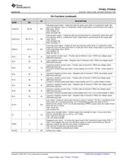
Power down – An active-low signal that controls the TFP401/401A power-down state. During
power down, all output buffers are switched to a high-impedance state. All analog circuits are
powered down and all inputs are disabled, except for PD.
PD 2 DI
If PD is left unconnected, an internal pullup defaults the TFP401/401A to normal operation.
High : Normal operation
Low: Power down
Output drive power down – An active-low signal that controls the power-down state of the
output drivers. During output drive power down, the output drivers (except SCDT and CTL1)
are driven to a high-impedance state. When PDO is left unconnected, an internal pullup
PDO 9 DI
defaults the TFP401/401A to normal operation.
High: Normal operation/output drivers on
Low: Output drive power down
PGND 98 GND PLL GND – Ground reference and current return for internal PLL
Pixel select – Selects between one- and two-pixels-per-clock output modes. During the 2-
pixel/clock mode, both even pixels, QE[23:0], and odd pixels, QO[23:0], are output in tandem
on a given clock cycle. During 1-pixel/clock, even and odd pixels are output sequentially, one
PIXS 4 DI at a time, with the even pixel first, on the even pixel bus, QE[23:0]. (The first pixel per line is
pixel-0, the even pixel. The second pixel per line is pixel-1, the odd pixel).
High: 2-pixel/clock
Low: 1-pixel/clock
PV
DD
97 V
DD
PLL V
DD
– Power supply for internal PLL
Even green-pixel output – Output for even and odd green pixels when in 1-pixel/clock mode.
Output for even-only green pixel when in 2-pixel/clock mode. Output data is synchronized to
QE[8:15] 20–27 DO the output data clock, ODCK.
LSB: QE8/pin 20
MSB: QE15/pin 27
Even red-pixel output – Output for even and odd red pixels when in 1-pixel/clock mode.
Output for even-only red pixel when in 2-pixel/clock mode. Output data is synchronized to the
QE[16:23] 30–37 DO output data clock, ODCK.
LSB: QE16/pin 30
MSB: QE23/pin 37
Odd blue-pixel output – Output for odd-only blue pixel when in 2-pixel/clock mode. Not used,
and held low, when in 1-pixel/clock mode. Output data is synchronized to the output data
QO[0:7] 49–56 DO clock, ODCK.
LSB: QO0/pin 49
MSB: QO7/pin 56
4 Submit Documentation Feedback Copyright © 2000–2015, Texas Instruments Incorporated
Product Folder Links: TFP401 TFP401A
器件 Datasheet 文档搜索
AiEMA 数据库涵盖高达 72,405,303 个元件的数据手册,每天更新 5,000 多个 PDF 文件
