Datasheet 搜索 > 稳压芯片 > TI(德州仪器) > TPS63020DSJR 数据手册 > TPS63020DSJR 数据手册 8/29 页

¥ 2.993
TPS63020DSJR 数据手册 - TI(德州仪器)
制造商:
TI(德州仪器)
分类:
稳压芯片
封装:
VSON-14
描述:
TEXAS INSTRUMENTS TPS63020DSJR 直流-直流开关降压, 升压稳压器, 可调, 1.8V-5.5V输入, 1.2V-5.5V/4A输出, 2.4MHz, VSON-14 新
Pictures:
3D模型
符号图
焊盘图
引脚图
产品图
页面导航:
引脚图在P3Hot
典型应用电路图在P1P12
原理图在P1P7P8
封装尺寸在P22P24P25
标记信息在P22
封装信息在P21P22P23P24P25
技术参数、封装参数在P3
应用领域在P1P29
电气规格在P5P9
导航目录
TPS63020DSJR数据手册
Page:
of 29 Go
若手册格式错乱,请下载阅览PDF原文件
_
+
PGND PGND
VIN
VOUT
+
-
VREF
PGND
PGND
FB
VOUT
L2L1
VIN
VINA
PS/SYNC
EN
GND
VINA
Current
Sensor
Gate
Control
Modulator
Oscillator
Device
Control
PG
Temperature
Control
_
+
TPS63020
,
TPS63021
SLVS916D –JULY 2010–REVISED OCTOBER 2015
www.ti.com
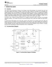
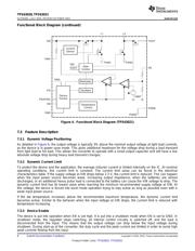
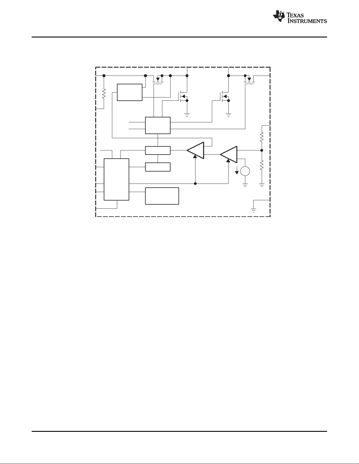
Functional Block Diagram (continued)
Figure 4. Functional Block Diagram (TPS63021)
7.3 Feature Description
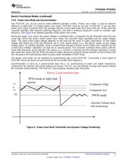
7.3.1 Dynamic Voltage Positioning
As detailed in Figure 6, the output voltage is typically 3% above the nominal output voltage at light load currents,
as the device is in power save mode. This gives additional headroom for the voltage drop during a load transient
from light load to full load. This allows the converter to operate with a small output capacitor and still have a low
absolute voltage drop during heavy load transient changes.
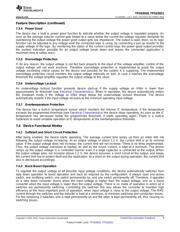
7.3.2 Dynamic Current Limit
To protect the device and the application, the average inductor current is limited internally on the IC. At nominal
operating conditions, this current limit is constant. The current limit value can be found in the electrical
characteristics table. If the supply voltage at VIN drops below 2.3 V, the current limit is reduced. This can happen
when the input power source becomes weak. Increasing output impedance, when the batteries are almost
discharged, or an additional heavy pulse load is connected to the battery can cause the VIN voltage to drop. The
dynamic current limit has its lowest value when reaching the minimum recommended supply voltage at VIN. At
this voltage, the device is forced into burst mode operation trying to stay active as long as possible even with a
weak input power source.
If the die temperature increases above the recommended maximum temperature, the dynamic current limit
becomes active. Similar to the behavior when the input voltage at VIN drops, the current limit is reduced with
temperature increasing.
7.3.3 Device Enable
The device is put into operation when EN is set high. It is put into a shutdown mode when EN is set to GND. In
shutdown mode, the regulator stops switching, all internal control circuitry is switched off, and the load is
disconnected from the input. This means that the output voltage can drop below the input voltage during
shutdown. During start-up of the converter, the duty cycle and the peak current are limited in order to avoid high
peak currents flowing from the input.
8 Submit Documentation Feedback Copyright © 2010–2015, Texas Instruments Incorporated
Product Folder Links: TPS63020 TPS63021
器件 Datasheet 文档搜索
AiEMA 数据库涵盖高达 72,405,303 个元件的数据手册,每天更新 5,000 多个 PDF 文件
