Datasheet 搜索 > FET驱动器 > TI(德州仪器) > UCC27511DBVR 数据手册 > UCC27511DBVR 数据手册 4/39 页

¥ 2.644
UCC27511DBVR 数据手册 - TI(德州仪器)
制造商:
TI(德州仪器)
分类:
FET驱动器
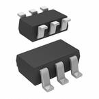
封装:
SOT-23-6
描述:
TEXAS INSTRUMENTS UCC27511DBVR 驱动器, IGBT, MOSFET, 低压侧, 4.5V-18V电源, 8A输出, -999ms 延迟, SOT-23-6
Pictures:
3D模型
符号图
焊盘图
引脚图
产品图
页面导航:
引脚图在P5P6Hot
典型应用电路图在P1P22P23P24P25P26
原理图在P15P16P17
封装尺寸在P30P32P33
标记信息在P30
封装信息在P7P29P30P31P32P33
功能描述在P4P5
技术参数、封装参数在P7
应用领域在P1P31P39
电气规格在P4P9P19P23
型号编号列表在P4
导航目录
UCC27511DBVR数据手册
Page:
of 39 Go
若手册格式错乱,请下载阅览PDF原文件
UCC27511
,
UCC27512
SLUSAW9F –FEBRUARY 2012–REVISED NOVEMBER 2014
www.ti.com
5 Description (Continued)
UCC27511 features a dual-input design which offers flexibility of implementing both inverting (IN– pin) and
noninverting (IN+ pin) configuration with the same device. Either IN+ or IN– pin can be used to control the state
of the driver output. The unused input pin can be used for enable and disable functions. For safety purpose,
internal pullup and pulldown resistors on the input pins ensure that outputs are held low when input pins are in
floating condition. Hence the unused input pin is not left floating and must be properly biased to ensure that
driver output is in enabled for normal operation.
The input pin threshold of the UCC27511 device is based on TTL and CMOS-compatible low-voltage logic which
is fixed and independent of the V
DD
supply voltage. Wide hysteresis between the high and low thresholds offers
excellent noise immunity.
The UCC27511 and UCC27512 provides 4-A source, 8-A sink (asymmetrical drive) peak-drive current capability.
Strong sink capability in asymmetrical drive boosts immunity against parasitic, Miller turnon effect. The
UCC27511 device also features a unique split output configuration where the gate-drive current is sourced
through OUTH pin and sunk through OUTL pin. This unique pin arrangement allows the user to apply
independent turnon and turnoff resistors to the OUTH and OUTL pins respectively and easily control the
switching slew rates.
UCC27511 and UCC27512 are designed to operate over a wide V
DD
range of 4.5 to 18 V and wide temperature
range of –40°C to 140°C. Internal Undervoltage Lockout (UVLO) circuitry on V
DD
pin holds output low outside
V
DD
operating range. The capability to operate at low voltage levels such as below 5 V, along with best-in-class
switching characteristics, is especially suited for driving emerging wide band-gap power-switching devices such
as GaN power-semiconductor devices.
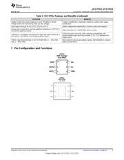
6 UCC2751x Product Family
The UCC2751x family of gate-driver products (Table 1) represent Texas Instruments’ latest generation of single-
channel low-side high-speed gate-driver devices featuring high-source/sink current capability, industry best-in-
class switching characteristics and a host of other features (Table 2) all of which combine to ensure efficient,
robust and reliable operation in high-frequency switching power circuits.
Table 1. UCC2751x Product Family Summary
PART NUMBER PACKAGE PEAK CURRENT
INPUT THRESHOLD LOGIC
(SOURCE/SINK)
UCC27511DBV SOT-23, 6 pin
4-A/8-A
CMOS/TTL-Compatible
(Asymmetrical Drive)
UCC27512DRS 3-mm x 3-mm WSON, 6 pin
(low voltage, independent of VDD
UCC27516DRS
(1)
3-mm x 3-mm WSON, 6 pin
bias voltage)
UCC27517DBV
(1)
SOT-23, 5 pin
4-A/4-A
(Symmetrical Drive)
UCC27518DBV
(1)
SOT-23, 5 pin
CMOS
(follows VDD bias voltage)
UCC27519DBV
(1)
SOT-23, 5 pin
(1) Visit www.ti.com for the latest product datasheet.
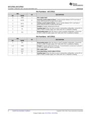
Table 2. UCC2751x Features and Benefits
FEATURE BENEFIT
High Source and Sink Current Capability High current capability offers flexibility in employing UCC2751x
4 A and 8 A (Asymmetrical) – UCC2751/6/7/8/9 family of devices to drive a variety of power switching devices at
4 A and 4 A (Symmetrical) – UCC27511 and UCC27512 varying speeds
Best-in-class 13-ns (typ) Propagation delay Extremely low pulse-transmission distortion
Expanded VDD Operating range of 4.5 V to 18 V
Flexibility in system design
Low VDD operation ensures compatibility with emerging wide band-
Expanded Operating Temperature range of –40°C to 140°C
gap power devices such as GaN
(See Electrical Characteristics table)
Outputs are held low in UVLO condition, which ensures predictable
VDD UVLO Protection
glitch-free operation at power up and power down
Safety feature, especially useful in passing abnormal condition tests
Outputs held low when input pins (INx) in floating condition
during safety certification
4 Submit Documentation Feedback Copyright © 2012–2014, Texas Instruments Incorporated
Product Folder Links: UCC27511 UCC27512
器件 Datasheet 文档搜索
AiEMA 数据库涵盖高达 72,405,303 个元件的数据手册,每天更新 5,000 多个 PDF 文件
