Datasheet 搜索 > FPGA芯片 > Altera(阿尔特拉) > 5CSEBA2U23C8SN 数据手册 > 5CSEBA2U23C8SN 其他数据使用手册 2/169 页

¥ 192.328
5CSEBA2U23C8SN 其他数据使用手册 - Altera(阿尔特拉)
制造商:
Altera(阿尔特拉)
分类:
FPGA芯片
封装:
UBGA-672
描述:
FPGA - 现场可编程门阵列 CycloneV SoC SE SNGL -core ARM Cortex-A9
Pictures:
3D模型
符号图
焊盘图
引脚图
产品图
页面导航:
原理图在P12P13P15P22P27P33
技术参数、封装参数在P132
应用领域在P164
导航目录
5CSEBA2U23C8SN数据手册
Page:
of 169 Go
若手册格式错乱,请下载阅览PDF原文件

Contents
Transceiver Architecture in Cyclone V Devices................................................. 1-1
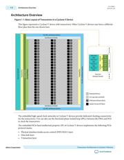
Architecture Overview................................................................................................................................ 1-2
Transceiver Banks............................................................................................................................1-3
6.144 Gbps CPRI Support Capability in GT Devices..................................................................1-8
Transceiver Channel Architecture.................................................................................................1-8
PMA Architecture........................................................................................................................................1-8
Transmitter PMA Datapath........................................................................................................... 1-9
Receiver PMA Datapath................................................................................................................1-16
Transmitter PLL.............................................................................................................................1-21
Clock Divider..................................................................................................................................1-26
Calibration Block........................................................................................................................... 1-27
PCS Architecture........................................................................................................................................1-29
Transmitter PCS Datapath........................................................................................................... 1-30
Receiver PCS Datapath..................................................................................................................1-36
Channel Bonding.......................................................................................................................................1-55
PLL Sharing................................................................................................................................................ 1-55
Document Revision History.....................................................................................................................1-55
Transceiver Clocking in Cyclone V Devices....................................................... 2-1
Input Reference Clocking...........................................................................................................................2-1
Dedicated Reference Clock Pins....................................................................................................2-2
Fractional PLL (fPLL)......................................................................................................................2-4
Internal Clocking......................................................................................................................................... 2-5
Transmitter Clock Network........................................................................................................... 2-6
Transmitter Clocking....................................................................................................................2-10
Receiver Clocking.......................................................................................................................... 2-15
FPGA Fabric–Transceiver Interface Clocking.......................................................................................2-18
Transceiver Datapath Interface Clocking...................................................................................2-21
Transmitter Datapath Interface Clocking..................................................................................2-21
Receiver Datapath Interface Clock..............................................................................................2-25
Document Revision History.....................................................................................................................2-29
Transceiver Reset Control in Cyclone V Devices............................................... 3-1
PHY IP Embedded Reset Controller.........................................................................................................3-1
Embedded Reset Controller Signals..............................................................................................3-1
Resetting the Transceiver with the PHY IP Embedded Reset Controller During Device
Power-Up.....................................................................................................................................3-3
Resetting the Transceiver with the PHY IP Embedded Reset Controller During Device
Operation.....................................................................................................................................3-4
User-Coded Reset Controller.....................................................................................................................3-5
User-Coded Reset Controller Signals............................................................................................3-6
TOC-2
Cyclone V Device Handbook Volume 2: Transceivers
Altera Corporation
器件 Datasheet 文档搜索
AiEMA 数据库涵盖高达 72,405,303 个元件的数据手册,每天更新 5,000 多个 PDF 文件
