Datasheet 搜索 > RAM芯片 > Cypress Semiconductor(赛普拉斯) > CY7C1049B15VXC 数据手册 > CY7C1049B15VXC 产品描述及参数 4/9 页


¥ 0
CY7C1049B15VXC 产品描述及参数 - Cypress Semiconductor(赛普拉斯)
制造商:
Cypress Semiconductor(赛普拉斯)
分类:
RAM芯片
Pictures:
3D模型
符号图
焊盘图
引脚图
产品图
页面导航:
引脚图在P1Hot
原理图在P1
型号编码规则在P7
功能描述在P1
导航目录
CY7C1049B15VXC数据手册
Page:
of 9 Go
若手册格式错乱,请下载阅览PDF原文件
CY7C1049B
Document #: 38-05169 Rev. *B Page 4 of 9
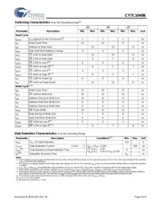
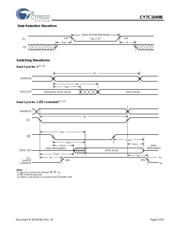
Switching Characteristics Over the Operating Range
[4]
-12 -15 -17
Parameter Description Min. Max. Min. Max. Min. Max. Unit
Read Cycle
t
power
V
CC
(typical) to the First Access
[5]
111ms
t
RC
Read Cycle Time 12 15 17 ns
t
AA
Address to Data Valid 121517ns
t
OHA
Data Hold from Address Change 3 3 3 ns
t
ACE
CE LOW to Data Valid 12 15 17 ns
t
DOE
OE LOW to Data Valid 6 7 8 ns
t
LZOE
OE LOW to Low Z
[7]
000ns
t
HZOE
OE HIGH to High Z
[6, 7]
677ns
t
LZCE
CE LOW to Low Z
[7]
333ns
t
HZCE
CE HIGH to High Z
[6, 7]
677ns
t
PU
CE LOW to Power-Up 0 0 0 ns
t
PD
CE HIGH to Power-Down 12 15 17 ns
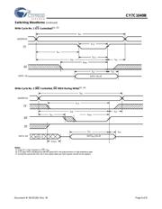
Write Cycle
[8, 9]
t
WC
Write Cycle Time 12 15 17 ns
t
SCE
CE LOW to Write End 10 12 12 ns
t
AW
Address Set-Up to Write End 10 12 12 ns
t
HA
Address Hold from Write End 0 0 0 ns
t
SA
Address Set-Up to Write Start 0 0 0 ns
t
PWE
WE Pulse Width 10 12 12 ns
t
SD
Data Set-Up to Write End 7 8 8 ns
t
HD
Data Hold from Write End 0 0 0 ns
t
LZWE
WE HIGH to Low Z
[7]
333ns
t
HZWE
WE LOW to High Z
[6, 7]
678ns
Data Retention Characteristics Over the Operating Range
Parameter Description Conditions
[11]
Min. Max. Unit
V
DR
V
CC
for Data Retention 2.0 V
I
CCDR
Data Retention Current Com’l L V
CC
= V
DR
= 2.0V,
CE
> V
CC
– 0.3V
V
IN
> V
CC
– 0.3V or V
IN
< 0.3V
200 µA
t
CDR
[3]
Chip Deselect to Data Retention Time 0 ns
t
R
[10]
Operation Recovery Time t
RC
ns
Notes:
4. Test conditions assume signal transition time of 3 ns or less, timing reference levels of 1.5V, input pulse levels of 0 to 3.0V, and output loading of the specified
I
OL
/I
OH
and 30-pF load capacitance.
5. This part has a voltage regulator which steps down the voltage from 5V to 3.3V internally. t
power
time has to be provided initially before a read/write operation
is started.
6. t
HZOE
, t
HZCE
, and t
HZWE
are specified with a load capacitance of 5 pF as in part (b) of AC Test Loads. Transition is measured ±500 mV from steady-state voltage.
7. At any given temperature and voltage condition, t
HZCE
is less than t
LZCE
, t
HZOE
is less than t
LZOE
, and t
HZWE
is less than t
LZWE
for any given device.
8. The internal write time of the memory is defined by the overlap of CE
LOW, and WE LOW. CE and WE must be LOW to initiate a write, and the transition of either of
these signals can terminate the write. The input data set-up and hold timing should be referenced to the leading edge of the signal that terminates the write.
9. The minimum write cycle time for Write Cycle no. 3 (WE
controlled, OE LOW) is the sum of t
HZWE
and t
SD
.
10.t
r
< 3 ns for all the speeds
11.No input may exceed V
CC
+ 0.5V.
器件 Datasheet 文档搜索
AiEMA 数据库涵盖高达 72,405,303 个元件的数据手册,每天更新 5,000 多个 PDF 文件
