Datasheet 搜索 > MOS管 > Fairchild(飞兆/仙童) > FCH041N65F_F085 数据手册 > FCH041N65F_F085 其他数据使用手册 1/9 页

¥ 48.618
FCH041N65F_F085 其他数据使用手册 - Fairchild(飞兆/仙童)
制造商:
Fairchild(飞兆/仙童)
分类:
MOS管
封装:
TO-247-3
Pictures:
3D模型
符号图
焊盘图
引脚图
产品图
页面导航:
型号编码规则在P1
标记信息在P1
技术参数、封装参数在P9
电气规格在P2

导航目录
FCH041N65F_F085数据手册
Page:
of 9 Go
若手册格式错乱,请下载阅览PDF原文件
November
2014
FCH041N65F_F085 N-Channel SuperFET II FRFET MOSFET
©2014 Fairchild Semiconductor Corporation
FCH041N65F_F085 Rev. B1
www.fairchildsemi.com1
FCH041N65F_F085
N-Channel SuperFET II FRFET MOSFET
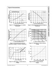
650 V, 76 A, 41 mΩ
Features
Typical R
DS(on)
= 34 mΩ at V
GS
= 10 V, I
D
= 38 A
Typical Q
g(tot)
= 234 nC at V
GS
= 10V, I
D
= 38 A
UIS Capability
Qualified to AEC Q101
RoHS Compliant
Description
SuperFET® II MOSFET is Fairchild Semiconductor’s brand-new
high voltage super-junction (SJ) MOSFET family that is utilizing
charge balance technology for outstanding low on-resistance
and lower gate charge performance. This technology is tailored
to minimize conduction loss,
provide superior switching
performance, dv/dt rate and higher avalanche energy.
Consequently SuperFETII is very well suited for the Soft switching
and Hard Switching topologies like High Voltage Full Bridge and
Half Bridge DC-DC, Interleaved Boost PFC, Boost PFC for HEV-EV
automotive.
SuperFET II FRFET® MOSFET’s optimized body diode reverse
recovery performance can remove additional component and
improve system reliability.
Application
Automotive On Board Charger
Automotive DC/DC converter for HEV
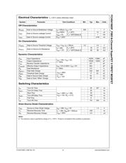
Maximum Ratings T
C
= 25°C unless otherwise noted
Symbol Parameter Ratings Units
V
DSS
Drain to Source Voltage 650 V
V
GS
Gate to Source Voltage ±20 V
I
D
T
C
= 25°C
Drain Current - Continuous (V
GS
=10) (Note 1) T
C
= 100°C
76 A
24 A
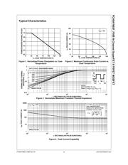
Pulsed Drain Current See Fig 4 A
E
AS
Si ngl e P uls e Av al an ch e R at ing (N ot e 2) 2025 mJ
dv/dt
MOSFET dv/dt 100
V/ns
Peak Diode Recovery dv/dt (Note 3) 50
P
D
Power Dissipation 595 W
Derate Above 25
o
C4.76W/
o
C
T
J
, T
STG
Operating and Storage Temperature -55 to + 150
o
C
R
θJC
M a x i m u m T h e r m a l R e s i s t a n c e J u n c t i o n t o C a s e 0 . 2 1
o
C/W
R
θJA
Maximum Thermal Resistance Junction to Ambient (Note 4) 40
o
C/W
Package Marking and Ordering Information
Device Marking Device Package Reel Size Tape Width Quantity
FCH041N65F FCH041N65F_F085 TO-247 - - 30
D
G
S
Forcurrentpackagedrawing,pleaserefertotheFairchildweb‐
siteathttps://www.fairchildsemi.com/package ‐drawings/TO/
TO247A03.pdf
Notes:
1: Current is limited by bondwire configuration.
2: Starting T
J
= 25°C, L = 18mH, I
AS
= 15A, V
DD
= 100V during inductor charging and V
DD
= 0V during time in avalanche.
3: I
SD
≤ 38A, di/dt ≤ 200 A/us, V
DD
≤ 380V, starting T
J
= 25°C.
4: R
θJA
is the sum of the junction-to-case and case-to-ambient thermal resistance, where the case thermal reference is defined as the solder
mounting surface of the drain pins. R
θJC
is guaranteed by design, while R
θJA
is determined by the board design. The maximum rating
presented here is based on mounting on a 1 in
2
pad of 2oz copper.
G
D
S
TO-247
器件 Datasheet 文档搜索
AiEMA 数据库涵盖高达 72,405,303 个元件的数据手册,每天更新 5,000 多个 PDF 文件
