Datasheet 搜索 > DC/DC转换器 > TI(德州仪器) > TPS62130ARGTR 数据手册 > TPS62130ARGTR 其他数据使用手册 6/46 页
 器件3D模型
¥ 1.518
TPS62130ARGTR 其他数据使用手册 - TI(德州仪器)
制造商:
TI(德州仪器)
分类:
DC/DC转换器
封装:
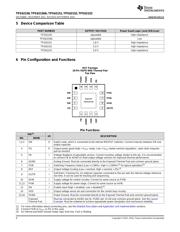
VQFN-16
描述:
TEXAS INSTRUMENTS TPS62130ARGTR 直流-直流开关降压, 逐步递降稳压器, 可调, 3V-17V输入, 900mV-6V/3A输出, 2.5MHz, VQFN-16 新
Pictures:
3D模型
符号图
焊盘图
引脚图
产品图
页面导航:
引脚图在P4Hot
典型应用电路图在P13
原理图在P8P9P17
封装尺寸在P34P38P40P41P43
焊盘布局在P35P44
标记信息在P38P39
封装信息在P38P39P40P41
技术参数、封装参数在P5
应用领域在P13
电气规格在P6P12

导航目录
TPS62130ARGTR数据手册
Page:
of 46 Go
若手册格式错乱,请下载阅览PDF原文件
6
TPS62150
,
TPS62150A
,
TPS62151
,
TPS62152
,
TPS62153
ZHCSB86D –NOVEMBER 2011–REVISED SEPTEMBER 2016
www.ti.com.cn
Copyright © 2011–2016, Texas Instruments Incorporated
(1) The device is still functional down to Undervoltage Lockout (see parameter V
UVLO
).
(2) Current into AVIN+PVIN pins.
(3) This is the static current limit. It can be temporarily higher in applications due to internal propagation delay (see Current-Limit and Short-
Circuit Protection section).
(4) This is the accuracy provided at the FB pin for the adjustable V
OUT
version (line and load regulation effects are not included). For the
fixed voltage versions the (internal) resistive divider is included.
(5) Line and load regulation depend on external component selection and layout (see 图 22 and 图 23).
7.5 Electrical Characteristics
over operating junction temperature (T
J
= -40°C to 125°C), typical values at VIN=12 V and T
A
=25°C (unless otherwise noted)
PARAMETER TEST CONDITIONS MIN NOM MAX UNIT
SUPPLY
V
IN
Input Voltage Range
(1)
3 17 V
I
Q
Operating Quiescent Current
EN = High, I
OUT
= 0 mA,
device not switching
17 30
µA
T
A
= -40°C to +85°C 17 25
I
SD
Shutdown Current
(2)
EN = Low
1.5 25
µA
T
A
= -40°C to +85°C 1.5 4
V
UVLO
Undervoltage Lockout Threshold
Falling Input Voltage (PWM mode operation) 2.6 2.7 2.8 V
Hysteresis 200 mV
T
SD
Thermal Shutdown Temperature 160
°C
Thermal Shutdown Hysteresis 20
CONTROL (EN, DEF, FSW, SS/TR, PG)
V
H
High Level Input Threshold Voltage (EN,
DEF, FSW)
0.9 0.65 V
V
L
Low Level Input Threshold Voltage (EN,
DEF, FSW)
0.45 0.3 V
I
LKG
Input Leakage Current (EN, DEF, FSW) EN = V
IN
or GND; DEF, FSW = V
OUT
or GND 0.01 1 µA
V
TH_PG
Power Good Threshold Voltage
Rising (%V
OUT
) 92% 95% 98%
Falling (%V
OUT
) 87% 90% 94%
V
OL_PG
Power Good Output Low Voltage I
PG
= –2 mA 0.07 0.3 V
I
LKG_PG
Input Leakage Current (PG) V
PG
= 1.8 V 1 400 nA
I
SS/TR
SS/TR Pin Source Current 2.3 2.5 2.7 µA
POWER SWITCH
r
DS(on)
High-Side MOSFET ON-Resistance
V
IN
≥ 6 V 90 170
mΩ
V
IN
= 3 V 120
Low-Side MOSFET ON-Resistance
V
IN
≥ 6 V 40 70
mΩ
V
IN
= 3 V 50
I
LIMF
High-Side MOSFET Forward Current
Limit
(3)
V
IN
= 12 V, T
A
= 25°C
1.4 1.7 2.2 A
OUTPUT
I
LKG_FB
Input Leakage Current (FB) TPS62150, V
FB
= 0.8 V 1 100 nA
V
OUT
Output Voltage Range (TPS62150) V
IN
≥ V
OUT
0.9 6.0 V
DEF (Output Voltage Programming)
DEF = 0 (GND) V
OUT
DEF = 1 (V
OUT
) V
OUT
+ 5%
Initial Output Voltage Accuracy
(4)
PWM mode operation, V
IN
≥ V
OUT
+ 1 V 785.6 800 814.4
mV
PWM mode operation, V
IN
≥ V
OUT
+ 1 V,
T
A
= –10°C to 85°C
788.0 800 812.8
Power Save Mode operation, C
OUT
= 22 µF 781.6 800 822.4
Load Regulation
(5)
V
IN
= 12 V, V
OUT
= 3.3 V, PWM mode
operation
0.05 %/A
Line Regulation
(5)
3 V ≤ V
IN
≤ 17 V, V
OUT
= 3.3 V, I
OUT
= 1 A,
PWM mode operation
0.02 %/V
器件 Datasheet 文档搜索
AiEMA 数据库涵盖高达 72,405,303 个元件的数据手册,每天更新 5,000 多个 PDF 文件
