Datasheet 搜索 > 稳压芯片 > ADI(亚德诺) > ADP7156ACPZ-3.3-R7 数据手册 > ADP7156ACPZ-3.3-R7 产品设计参考手册 5/8 页
 器件3D模型
¥ 37.511
ADP7156ACPZ-3.3-R7 产品设计参考手册 - ADI(亚德诺)
制造商:
ADI(亚德诺)
分类:
稳压芯片
封装:
LFCSP-10
描述:
低压差稳压器 3.3/5Vin 1.2A Ultra Low Noise LDO, Fixed
Pictures:
3D模型
符号图
焊盘图
引脚图
产品图
页面导航:
原理图在P3
型号编码规则在P8
导航目录
ADP7156ACPZ-3.3-R7数据手册
Page:
of 8 Go
若手册格式错乱,请下载阅览PDF原文件

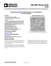
EVAL-ADP7156 User Guide UG-809
Rev. 0 | Page 5 of 8
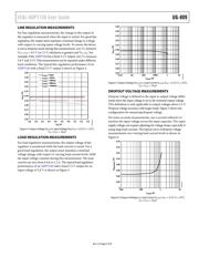
LINE REGULATION MEASUREMENTS
For line regulation measurements, the change in the output of
the regulator is measured when the input is varied. For good line
regulation, the output must maintain a minimal change in voltage
with respect to varying input voltage levels. To ensure the device
is not in dropout mode during this measurement, vary V
IN
between
V
OUT_NOM
+ 0.5 V (or 2.3 V, whichever is greater) and V
IN_MAX
. For
example, if the ADP7156 has a fixed 3.3 V output, vary V
IN
between
3.8 V and 5.5 V. This measurement can be repeated under different
load conditions. The typical line regulation performance of an
ADP7156 with a fixed 3.3 V output is shown in Figure 4.
V
OUT
(V)
I
L
O
AD
= 0mA
I
L
OA
D
= 10mA
I
LOAD
= 100mA
I
LOAD
=
600
m
A
I
L
OAD
=
120
0m
A
3.8 4.0
4.2 4.4 4.6 4.8 5.0
5.45.2
5.6
V
IN
(V)
12948-006
3.25
3.26
3.27
3.28
3.29
3.30
3.31
3.32
3.33
3.34
3.35
Figure 4. Output Voltage (V
OUT
) vs. Input Voltage (V
IN
), V
OUT
= 3.3 V, T
A
= 25°C,
C
IN
= C
OUT
= 10 µF
LOAD REGULATION MEASUREMENTS
For load regulation measurements, the output voltage of the
regulator is monitored while the load current is varied. For a
good load regulation, the output must maintain a minimal
voltage change with respect to varying load current levels. Hold
the input voltage constant during this measurement. The load
current can vary from 0 mA to 1.2 A. The typical load regulation
performance of an ADP7156 with a fixed 3.3 V output for an
input voltage of 3.8 V is shown in Figure 5.
3.25
3.26
3.27
3.28
3.29
3.30
3.31
3.32
3.33
3.34
3.35
0.1m 1m 10m 100m 1 10
V
OUT
(V)
I
LOAD
(A)
12948-007
Figure 5. Output Voltage (V
OUT
) vs. Load Current (I
LOAD
), V
OUT
= 3.3 V, T
A
= 25°C,
C
IN
= C
OUT
= 10 µF
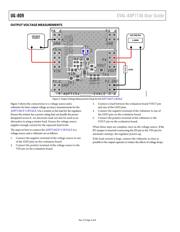
DROPOUT VOLTAGE MEASUREMENTS
Dropout voltage is defined as the input to output voltage differ-
ential when the input voltage is set to the nominal output voltage.
This definition is only applicable to output voltages above 2.3 V.
Dropout voltage increases with larger loads. Figure 3 shows the
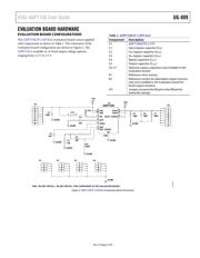
configuration for measuring dropout voltage.
For more accurate measurements, use a second voltmeter to
monitor the input voltage across the input capacitor. The input
supply voltage can require adjusting for voltage drops, especially if
using large load currents. The typical curve of dropout voltage
measurements over varying load current levels is shown in
Figure 6.
12948-008
0
0.16
0.14
0.12
0.10
0.08
0.06
0.04
0.02
10m 100 1 10
V
DROPOUT
(V)
I
LOAD
(A)
Figure 6. Dropout Voltage vs. Load Current (I
LOAD
), V
OUT
= 3.3 V, T
A
= 25°C,
C
IN
= C
OUT
= 10 µF
器件 Datasheet 文档搜索
AiEMA 数据库涵盖高达 72,405,303 个元件的数据手册,每天更新 5,000 多个 PDF 文件
