Datasheet 搜索 > Avnet > AFT05MP075GNR1 数据手册 > AFT05MP075GNR1 开发手册 4/21 页


¥ 0
AFT05MP075GNR1 开发手册 - Avnet
制造商:
Avnet
Pictures:
3D模型
符号图
焊盘图
引脚图
产品图
页面导航:
导航目录
AFT05MP075GNR1数据手册
Page:
of 21 Go
若手册格式错乱,请下载阅览PDF原文件
4
RF Device Data
Freescale Semiconductor, Inc.
AFT05MP075NR1 AFT05MP075GNR1
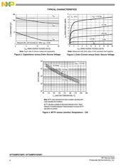
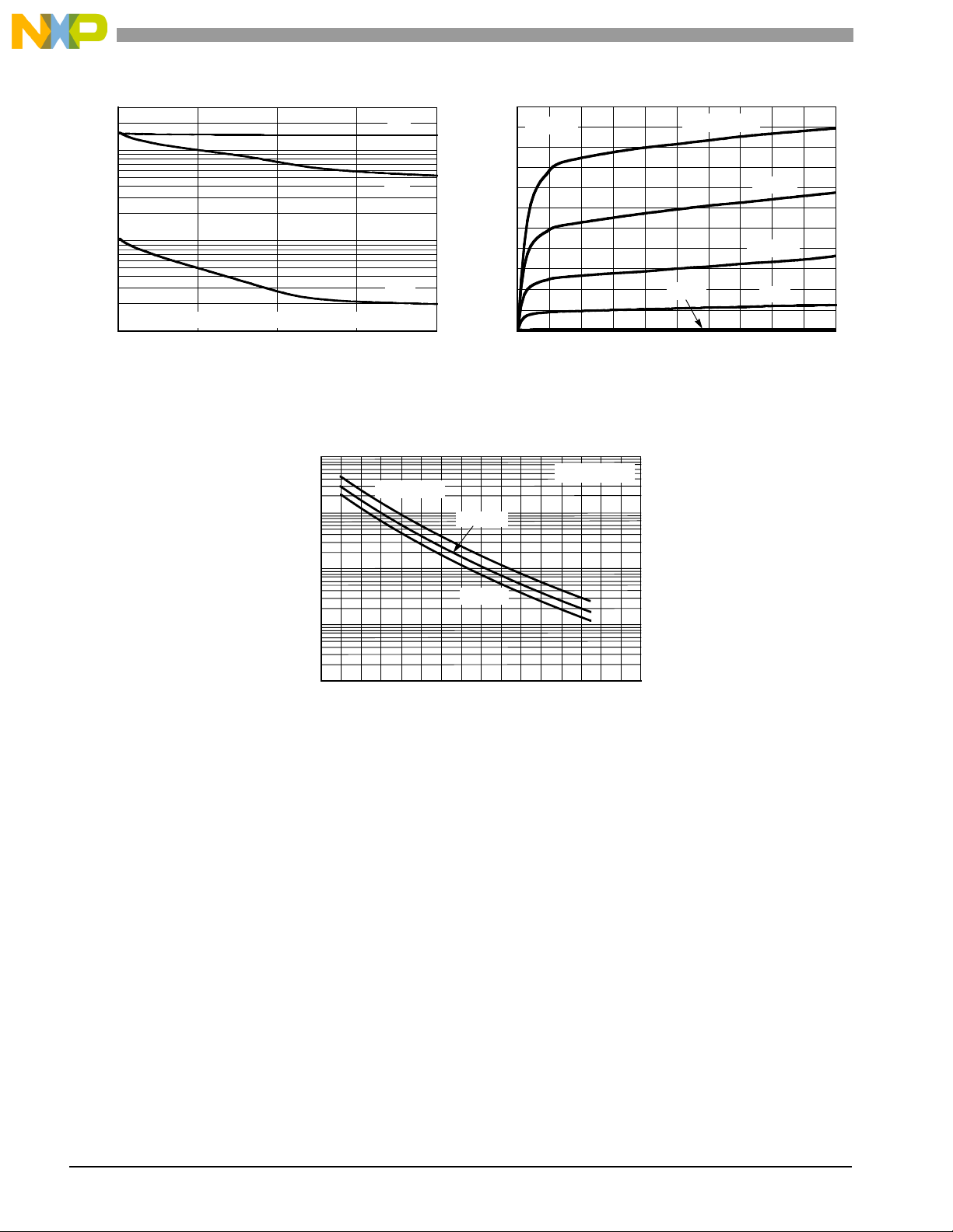
TYPICAL CHARACTERISTICS
20
1
300
0105
V
DS
, DRAIN--SOURCE VOLTAGE (VOLTS)
Figure 2. Capacitance versus Drain--Source Voltage
C, CAPACITANCE (pF)
10
15
100
Measured with 30 mV(rms)ac @ 1 MHz, V
GS
=0Vdc
C
rss
C
iss
C
oss
0
5
4
V
DS
, DRAIN--SOURCE VOLTAGE (VOLTS)
Figure 3. Drain Current versus D rain--Source Voltage
2
V
GS
=3.75Vdc
Note: Measured with both sides of the transistor tied together.
4
3
1
8121620
I
DS
, DRAIN CURRENT (AMPS)
3Vdc
T
A
=25C
2.5 Vdc
25090
T
J
, JUNCTION TEMPERATURE (C)
Figure 4. MTTF versus Junction Temperature -- CW
Note: MTTF value represents the total cumulative operating time
under indicated test conditions.
MTTF calculator available at http://www.freescale.com/rf. Select
Software & Tools/Development Tools/Calculators to access MTTF
calculators by product.
10
7
10
6
10
4
110 130 150 170 190
MTTF (HOURS)
210 230
10
8
10
5
0
6
7
V
DD
= 12.5 Vdc
I
D
=6.3Amps
9.4 Amps
7.8 Amps
3.5 Vdc
3.25 Vdc
9
8
10
11
2 6 10 14 18
Note: Each side of device measured separately.
器件 Datasheet 文档搜索
AiEMA 数据库涵盖高达 72,405,303 个元件的数据手册,每天更新 5,000 多个 PDF 文件
