Datasheet 搜索 > 时钟信号器件 > ADI(亚德诺) > AD9548BCPZ-REEL7 数据手册 > AD9548BCPZ-REEL7 数据手册 32/111 页
 器件3D模型
¥ 335.917
AD9548BCPZ-REEL7 数据手册 - ADI(亚德诺)
制造商:
ADI(亚德诺)
分类:
时钟信号器件
封装:
LFCSP-88
描述:
四路/八路输入网络时钟发生器/同步器 Quad/Octal Input Network Clock Generator/Synchronizer
Pictures:
3D模型
符号图
焊盘图
引脚图
产品图
页面导航:
引脚图在P15P33P51P111Hot
典型应用电路图在P46P51
原理图在P1P26P31P35P38P39P43
封装尺寸在P111
型号编码规则在P111
功能描述在P1P15P37P111
技术参数、封装参数在P1P4P8P10P11P14P106
应用领域在P1P37
电气规格在P18
导航目录
AD9548BCPZ-REEL7数据手册
Page:
of 111 Go
若手册格式错乱,请下载阅览PDF原文件
AD9548 Data Sheet
Rev. G | Page 32 of 111
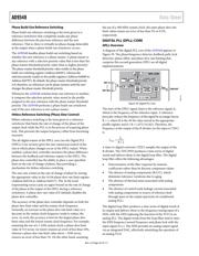
Phase Build-Out Reference Switching
Phase build-out reference switching is the term given to a
reference switchover that completely masks any phase
difference between the previous reference and the new
reference. That is, there is virtually no phase change detectable
at the output when a phase build-out switchover occurs.
The AD9548 handles phase build-out switching based on
whether the new reference is a phase master. A phase master is
any reference with a selection priority value that is less than the
phase master threshold priority value (that is, higher priority).
The phase master threshold priority value resides in the phase
build-out switching register (Address 0x0507), whereas the
selection priority resides in the profile registers (Address 0x0600 to
Address 0x07FF). By default, the phase master threshold priority
is 0; therefore, no references can be phase masters until the user
changes the phase master threshold priority.
Whenever the AD9548 switches from one reference to another,
it compares the selection priority value stored in the profile
assigned to the new reference with the phase master threshold
priority. The AD9548 performs a phase build-out switchover
only if the new reference is not a phase master.
Hitless Reference Switching (Phase Slew Control)
Hitless reference switching is the term given to a reference
switchover that limits the rate of change of the phase of the
output clock while the PLL is in the process of acquiring phase
lock. This prevents the output frequency offset from becoming
excessive.
The all-digital nature of the DPLL core (see the Digital PLL
(DPLL) Core section) gives the user numerical control of the
rate at which phase changes occur at the DPLL output. When
enabled, a phase slew controller monitors the phase difference
between the feedback and reference inputs to the DPLL. The
phase slew controller has the ability to place a user specified
limit on the rate of change of phase, thus providing a
mechanism for hitless reference switching.
The user sets a limit on the rate of change of phase by storing
the appropriate value in the 16-bit phase slew rate limit register
(Address 0x0316 to Address 0x0317). The 16-bit word
(representing ns/sec) puts an upper bound on the rate of change
of the phase at the output of the DPLL during a reference
switchover. A phase slew rate value of 0 (default) disables the
phase slew controller.
The accuracy of the phase slew controller depends on both the
phase slew limit value and the system clock frequency.
Generally, an increase in the phase slew rate limit value or a
decrease in the system clock frequency tends to reduce the
error. As such, the accuracy is best for the largest phase slew
limit value and the lowest system clock frequency. For example,
assuming the use of a 1 GHz system clock, a phase slew limit
value of 315 ns/sec (or more) ensures an error of less than 10%,
whereas a phase slew rate limit value above ~3100 ns/sec
ensures an error of less than 1%. On the other hand, assuming
the use of a 500 MHz system clock, the same phase slew rate
limit values ensure an error of less than 5% or 0.5%,
respectively.
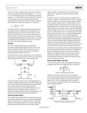
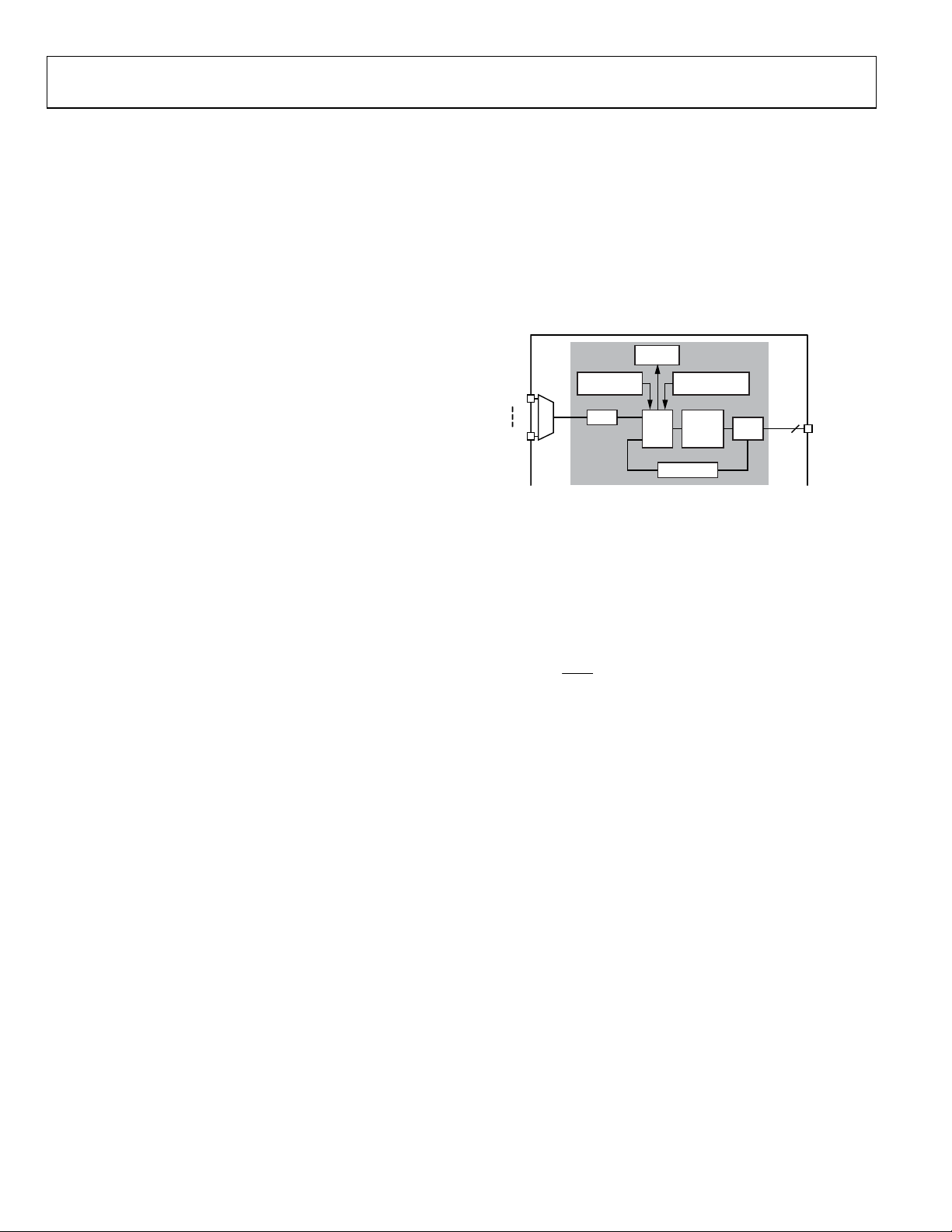
DIGITAL PLL (DPLL) CORE
DPLL Overview
A diagram of the digital PLL core of the AD9548 appears in
Figure 39. The phase/frequency detector, feedback path, lock
detectors, phase offset, and phase slew rate limiting that
comprise this second generation DPLL are all digital
implementations.
R
+
1
REF A
TDC
AND
PFD
DIGITAL
LOOP
FILTER
DDS/
DAC
DACOUT
CLOSED-LOOP
PHASE OFFSET
PHASE SLEW
LIMIT
LOCK
DETECT
REF DD
DPPL CORE
2
f
R
f
TDC
f
DDS
S + 1 + U/V
08022-013
Figure 39. Digital PLL Core
The start of the DPLL signal chain is the reference signal, f
R
,
which is the frequency of the reference input. A reference
prescaler reduces the frequency of this signal by an integer factor,
R + 1, where R is the 30-bit value stored in the appropriate
profile register and 0 ≤ R ≤ 1,073,741,823. Therefore, the
frequency at the output of the R-divider (or the input to TDC)
is
1
R
f
f
R
TDC
A time-to-digital converter (TDC) samples the output of the
R-divider. The TDC/PFD produces a time series of digital
words and delivers them to the digital loop filter. The digital
loop filter offers the following advantages:
Determination of the filter response by numeric
coefficients rather than by discrete component values
The absence of analog components (R/L/C), which
eliminates tolerance variations due to aging
The absence of thermal noise associated with analog
components
The absence of control node leakage current associated
with analog components (a source of reference feed-
through spurs in the output spectrum of a traditional
analog PLL)
The digital loop filter produces a time series of digital words at
its output and delivers them to the frequency tuning input of a
DDS, with the DDS replacing the function of the VCO in an
analog PLL. The digital words from the loop filter tend to steer
the DDS frequency toward frequency and phase lock with the
input signal (f
TDC
). The DDS provides an analog output signal
via an integrated DAC, effectively mimicking the operation of
an analog VCO.
器件 Datasheet 文档搜索
AiEMA 数据库涵盖高达 72,405,303 个元件的数据手册,每天更新 5,000 多个 PDF 文件
