Datasheet 搜索 > 时钟信号器件 > ADI(亚德诺) > AD9548BCPZ-REEL7 数据手册 > AD9548BCPZ-REEL7 数据手册 33/111 页
 器件3D模型
¥ 335.88
AD9548BCPZ-REEL7 数据手册 - ADI(亚德诺)
制造商:
ADI(亚德诺)
分类:
时钟信号器件
封装:
LFCSP-88
描述:
四路/八路输入网络时钟发生器/同步器 Quad/Octal Input Network Clock Generator/Synchronizer
Pictures:
3D模型
符号图
焊盘图
引脚图
产品图
页面导航:
引脚图在P15P33P51P111Hot
典型应用电路图在P46P51
原理图在P1P26P31P35P38P39P43
封装尺寸在P111
型号编码规则在P111
功能描述在P1P15P37P111
技术参数、封装参数在P1P4P8P10P11P14P106
应用领域在P1P37
电气规格在P18
导航目录
AD9548BCPZ-REEL7数据手册
Page:
of 111 Go
若手册格式错乱,请下载阅览PDF原文件
Data Sheet AD9548
Rev. G | Page 33 of 111
The DPLL includes a feedback divider that causes the DDS to
operate at an integer-plus-fractional multiple (S + 1 + U/V) of
f
TDC
. S is the 30-bit value stored in the profile register and has a
range of 7 ≤ S ≤ 1,073,741,823. U and V are the 10-bit numerator
and denominator values of the optional fractional divide
component and are also stored in the profile register. Together
they establish the nominal DDS frequency (f
DDS
), given by
V
U
S
R
f
f
R
DDS
1
1
Normally, fractional-N designs exhibit distinctive phase noise
and spurious artifacts resulting from the modulation of the
integer divider based on the fractional value. Such is not the
case for the AD9548 because it uses a purely digital means to
determine phase errors. Because the phase errors incurred by
modulating the feedback divider are deterministic, it is possible
to compensate for them digitally. The result is a fractional-N
PLL with no discernable modulation artifacts.
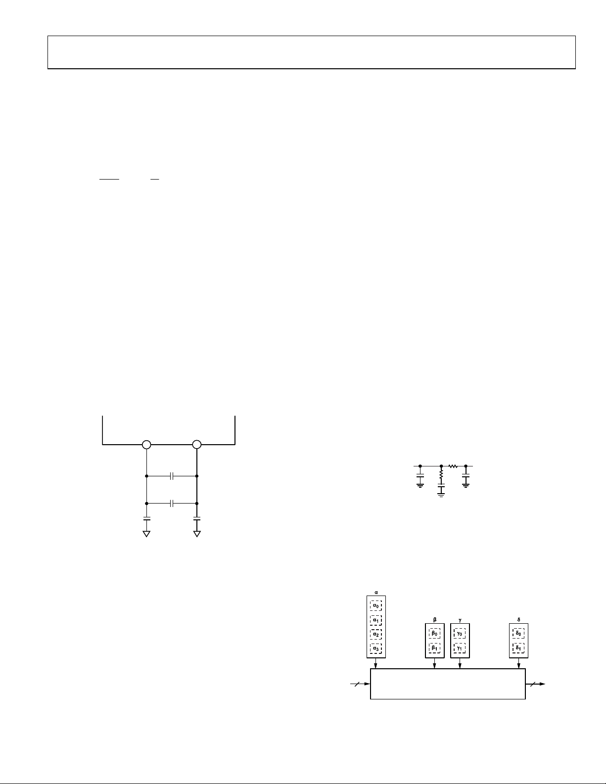
TDC/PFD
The TDC is a highly integrated functional block that
incorporates both analog and digital circuitry. There are two
pins associated with the TDC that the user must connect to
external components. Figure 40 shows the recommended
component values and their connections.
For best performance, place components as close as possible to
the device pins. Components with low effective series resistance
(ESR) and low parasitic inductance yield the best results.
AD9548
10µF
0.1µF
0.1µF
0.1µF
TDC_VRTTDC_VRB
58
57
08022-014
Figure 40. TDC Pin Connections
The phase-frequency detector (PFD) is an all-digital block. It
compares the digital output from the TDC (which relates to the
active reference edge) with the digital word from the feedback
block (which relates to the rollover edge of the DDS
accumulator after division by the feedback divider). It uses a
digital code pump and digital integrator (rather than a
conventional charge pump and capacitor) to generate the error
signal that steers the DDS frequency toward phase lock.
Closed-Loop Phase Offset
The all-digital nature of the TDC/PFD provides for numerical
control of the phase offset between the reference and feedback
edges. This allows the user to adjust the relative timing of the
distribution output edges relative to the reference input edges
by programming the 40-bit fixed phase lock offset register
(Address 0x030F to Address 0x0313). The 40-bit word is a
signed (twos complement) number that represents units of
picoseconds.
In addition, the user can adjust the closed-loop phase offset
(positive or negative) in incremental fashion. To do so, program
the desired step size in the 16-bit incremental phase lock offset
step size register (Address 0x0314 to Address 0x0315). This is
an unsigned number that represents units of picoseconds. The
programmed step size is added to the current closed-loop phase
offset each time the user writes a Logic 1 to the increment phase
offset bit (Register 0x0A0C, Bit 0). Conversely, the programmed
step size is subtracted from the current closed-loop phase offset
each time the user writes a Logic 1 to the decrement phase offset
bit (Register 0x0A0C, Bit 1). The serial input/output port
control logic clears both of these bits automatically. The user can
remove the incrementally accumulated phase by writing a Logic 1
to the reset incremental phase offset bit (Register 0x0A0C, Bit 2),
which is also cleared automatically. Alternatively, rather than
using the serial input/output port, the multifunction pins can be
set up to perform the increment, decrement, and clear functions.
Note that the incremental phase offset is completely independent of
the offset programmed into the fixed phase lock offset register.
However, if the phase slew limiter is active (see the Hitless
Reference Switching (Phase Slew Control) section), then any
instantaneous change in closed-loop phase offset (fixed or
incremental) will be subject to possible slew limitation by the
action of the phase slew limiter.
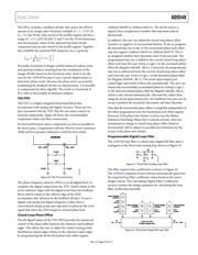
Programmable Digital Loop Filter
The AD9548 loop filter is a third order digital IIR filter that is
analogous to the third order analog loop shown in Figure 41.
C
3
C
2
C
1
R
2
R
3
08022-015
Figure 41. Third Order Analog Loop Filter
The filter requires four coefficients as shown in Figure 42.
The AD9548 evaluation board software automatically generates
the required loop filter coefficient values based on the user’s
design criteria. The Calculating Digital Filter Coefficients
section contains the design equations for calculating the loop
filter coefficients manually.
LOOP FILTER
(THIRD ORDER IIR)
IN OUT
FRACTIONAL
(16-BIT)
1/2
x
(6-BIT)
2
x
(3-BIT)
2
x
(4-BIT)
FRACTIONAL
(17-BIT)
1/2
x
(6-BIT)
FRACTIONAL
(17-BIT)
1/2
x
(6-BIT)
FRACTIONAL
(15-BIT)
1/2
x
(5-BIT)
4851
08022-016
Figure 42. Third Order Digital IIR Loop Filter
器件 Datasheet 文档搜索
AiEMA 数据库涵盖高达 72,405,303 个元件的数据手册,每天更新 5,000 多个 PDF 文件
