Datasheet 搜索 > 时钟信号器件 > ADI(亚德诺) > AD9548BCPZ-REEL7 数据手册 > AD9548BCPZ-REEL7 数据手册 35/111 页
 器件3D模型
¥ 335.88
AD9548BCPZ-REEL7 数据手册 - ADI(亚德诺)
制造商:
ADI(亚德诺)
分类:
时钟信号器件
封装:
LFCSP-88
描述:
四路/八路输入网络时钟发生器/同步器 Quad/Octal Input Network Clock Generator/Synchronizer
Pictures:
3D模型
符号图
焊盘图
引脚图
产品图
页面导航:
引脚图在P15P33P51P111Hot
典型应用电路图在P46P51
原理图在P1P26P31P35P38P39P43
封装尺寸在P111
型号编码规则在P111
功能描述在P1P15P37P111
技术参数、封装参数在P1P4P8P10P11P14P106
应用领域在P1P37
电气规格在P18
导航目录
AD9548BCPZ-REEL7数据手册
Page:
of 111 Go
若手册格式错乱,请下载阅览PDF原文件
Data Sheet AD9548
Rev. G | Page 35 of 111
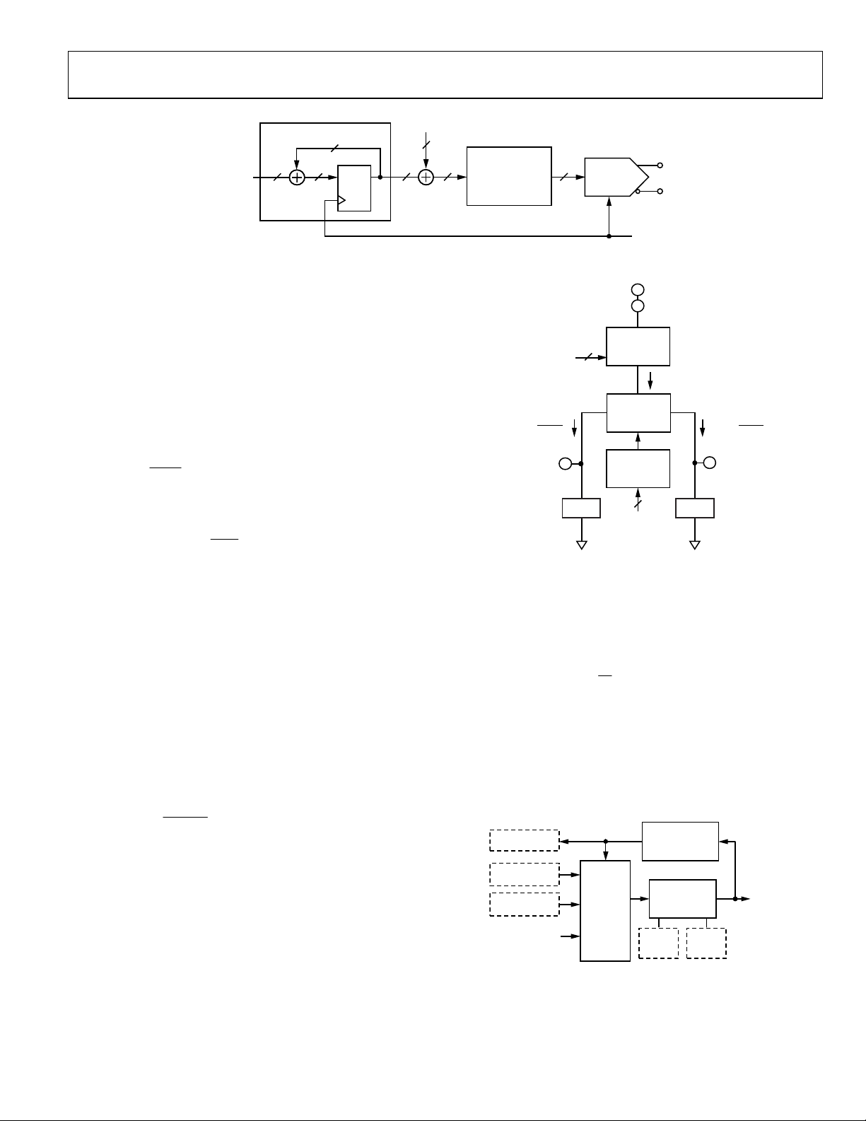
DAC
(14-BIT)
PHASE
OFFSET
QD
f
S
FREQUENCY
T
UNING WORD
(FTW)
DAC+
DAC–
1419
48
19
ANGLE TO
AMPLITUDE
CONVERSION
4848
48-BIT ACCUMULATOR
16
0
8022-018
Figure 44. DDS Block Diagram
The input to the DDS is the 48-bit FTW. The FTW serves as a
step size value. On each cycle of f
S
, the accumulator adds the
value of the FTW to the running total at its output. For
example, given FTW = 5, the accumulator counts by fives,
incrementing on each f
S
cycle. Over time, the accumulator
reaches the upper end of its capacity (2
48
in this case), at which
point, it rolls over but retains the excess. The average rate at
which the accumulator rolls over establishes the frequency of
the output sinusoid. The average rollover rate of the accumulator
establishes the output frequency (f
DDS
) of the DDS and is given by
SDDS
f
FTW
f
48
2
Solving this equation for FTW yields
S
DDS
f
f
FTW
48
2round
For example, given that f
S
= 1 GHz and f
DDS
= 155.52 MHz, then
FTW = 43,774,988,378,041 (0x27D028A1DFB9).
Note that the minimum DAC output frequency is 62.5 MHz;
therefore, normal operation requires an FTW that yields an
output frequency in excess of this lower bound.
DDS Phase Offset
The relative phase of the sinusoid generated by the DDS is
numerically controlled by adding a phase offset word to the output
of the DDS accumulator. This is accomplished via the open-loop
phase offset register (Address 0x030D to Address 0x030E),
which is a programmable 16-bit value (Δphase). The resulting
phase offset, ΔΦ (in radians), is given by
16
2
2Φ
phase
Phase offset and relative time offset are directly related. The
time offset is (
phase/2
16
)/f
DDS
(in seconds), where f
DDS
is the
output frequency of the DDS (in hertz).
DAC Output
The output of the digital core of the DDS is a time series of
numbers representing a sinusoidal waveform. The DAC
translates the numeric values to an analog signal. The DAC
output signal appears at two pins that constitute a balanced
current source architecture (see Figure 45).
CURRENT
SWITCH
ARRAY
SWITCH
CONTROL
I
FS
I
SCALE
AVDD3
DACOUTP DACOUTN
CURRENT
MIRROR
GND
21
22
GND
18
19
CODE
08022-019
CODE
50Ω50Ω
14
10
I
FS
(1– )
2
14
– 1
CODE
I
FS
( )
2
14
– 1
Figure 45. DAC Output Pins
The value of I
FS
is programmable via the 10-bit DAC full-scale
current word in the DAC current register (Address 0x0213 to
Address 0x0214). The value of the 10-bit word (I
SCALE
) sets I
FS
according to the following formula:
SCALE
I
16
3
72μA120
FS
I
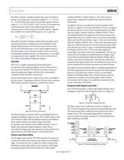
TUNING WORD PROCESSING
The frequency tuning words that dictate the output frequency
of the DDS come from one of three sources (see Figure 46).
The free running frequency tuning word register
The output of the digital loop filter
The output of the tuning word history processor
08022-070
TUNING WORD
HISTORY
PROCESSOR
TUNING WORD
HISTORY
FREE-RUN
TUNING WORD
TUNING WORD
UPDATE
FROM DIGITAL
LOOP FILTER
TO DDS
TUNING
WORD
ROUTING
CONTROL
TUNING
WORD
CLAMP
LOWER
TUNING
WORD
UPPER
TUNING
WORD
Figure 46. Tuning Word Processing
器件 Datasheet 文档搜索
AiEMA 数据库涵盖高达 72,405,303 个元件的数据手册,每天更新 5,000 多个 PDF 文件
