Datasheet 搜索 > AD转换器 > TI(德州仪器) > ADC124S101CIMMX/NOPB 数据手册 > ADC124S101CIMMX/NOPB 数据手册 2/27 页
 器件3D模型
¥ 44.272
ADC124S101CIMMX/NOPB 数据手册 - TI(德州仪器)
制造商:
TI(德州仪器)
分类:
AD转换器
封装:
VSSOP-10
描述:
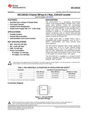
4 通道、500 ksps 至 1MSPS、12 位模数转换器 10-VSSOP -40 to 85
Pictures:
3D模型
符号图
焊盘图
引脚图
产品图
页面导航:
引脚图在P2Hot
典型应用电路图在P18
原理图在P2
封装尺寸在P22P24P25
标记信息在P22
封装信息在P22P23P24P25
焊接温度在P3
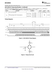
技术参数、封装参数在P1P3P5P6P17
应用领域在P1P16
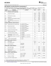
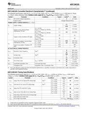
电气规格在P3P4P5P9P10P11P12P13P14P15P19
导航目录
ADC124S101CIMMX/NOPB数据手册
Page:
of 27 Go
若手册格式错乱,请下载阅览PDF原文件
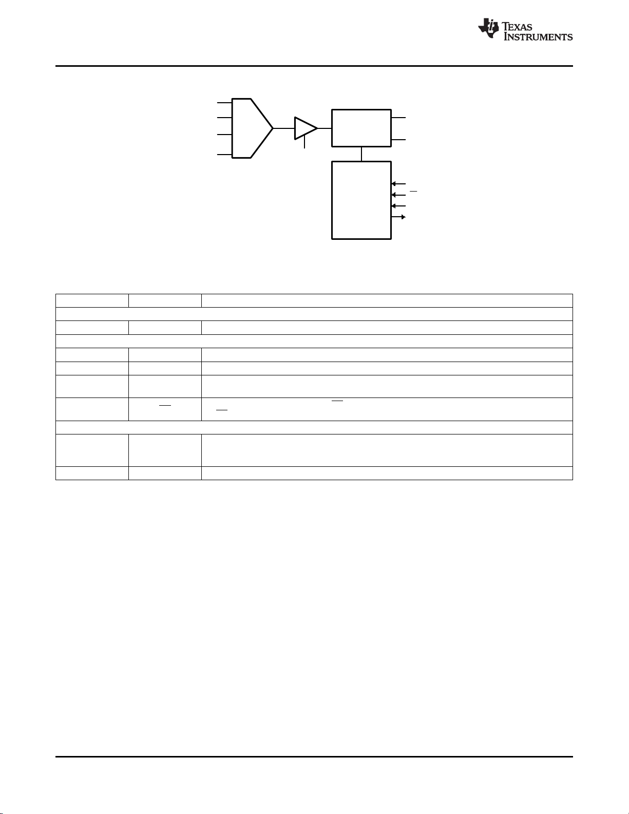
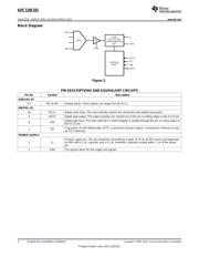
IN1
IN4
MUX
T/H
SCLK
V
A
GND
CS
DIN
DOUT
CONTROL
LOGIC
12-Bit
SUCCESSIVE
APPROXIMATION
ADC
.
.
.
GND
ADC124S101
SNAS283D –MARCH 2005–REVISED MARCH 2013
www.ti.com
Block Diagram
Figure 2.
PIN DESCRIPTIONS AND EQUIVALENT CIRCUITS
Pin No. Symbol Description
ANALOG I/O
4-7 IN1 to IN4 Analog inputs. These signals can range from 0V to V
A
.
DIGITAL I/O
10 SCLK Digital clock input. This clock directly controls the conversion and readout processes.
9 DOUT Digital data output. The output samples are clocked out of this pin on falling edges of the SCLK pin.
Digital data input. The ADC124S101's Control Register is loaded through this pin on rising edges of
8 DIN
the SCLK pin.
Chip select. On the falling edge of CS, a conversion process begins. Conversions continue as long
1 CS
as CS is held low.
POWER SUPPLY
Positive supply pin. This pin should be connected to a quiet +2.7V to +5.25V source and bypassed
2 V
A
to GND with a 1 µF capacitor and a 0.1 µF monolithic capacitor located within 1 cm of the power
pin.
3 GND The ground return for the supply and signals.
2 Submit Documentation Feedback Copyright © 2005–2013, Texas Instruments Incorporated
Product Folder Links: ADC124S101
器件 Datasheet 文档搜索
AiEMA 数据库涵盖高达 72,405,303 个元件的数据手册,每天更新 5,000 多个 PDF 文件
