Datasheet 搜索 > AD转换器 > TI(德州仪器) > ADC124S101CIMMX/NOPB 数据手册 > ADC124S101CIMMX/NOPB 数据手册 3/27 页
 器件3D模型
¥ 44.272
ADC124S101CIMMX/NOPB 数据手册 - TI(德州仪器)
制造商:
TI(德州仪器)
分类:
AD转换器
封装:
VSSOP-10
描述:
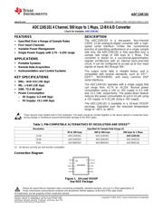
4 通道、500 ksps 至 1MSPS、12 位模数转换器 10-VSSOP -40 to 85
Pictures:
3D模型
符号图
焊盘图
引脚图
产品图
页面导航:
引脚图在P2Hot
典型应用电路图在P18
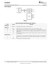
原理图在P2
封装尺寸在P22P24P25
标记信息在P22
封装信息在P22P23P24P25
焊接温度在P3
技术参数、封装参数在P1P3P5P6P17
应用领域在P1P16
电气规格在P3P4P5P9P10P11P12P13P14P15P19
导航目录
ADC124S101CIMMX/NOPB数据手册
Page:
of 27 Go
若手册格式错乱,请下载阅览PDF原文件
ADC124S101
www.ti.com
SNAS283D –MARCH 2005–REVISED MARCH 2013
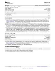
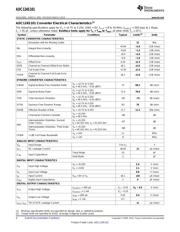
Absolute Maximum Ratings
(1)(2)(3)
Supply Voltage V
A
−0.3V to 6.5V
Voltage on Any Pin to GND −0.3V to V
A
+0.3V
Input Current at Any Pin
(4)
±10 mA
Package Input Current
(4)
±20 mA
Power Consumption at T
A
= 25°C See
(5)
ESD Susceptibility
(6)
Human Body Model 2500V
Machine Model 250V
Junction Temperature +150°C
Storage Temperature −65°C to +150°C
(1) Absolute Maximum Ratings indicate limits beyond which damage to the device may occur. Operating Ratings indicate conditions for
which the device is functional, but do not ensure specific performance limits. For ensured specifications and test conditions, see the
Electrical Characteristics. The ensured specifications apply only for the test conditions listed. Some performance characteristics may
degrade when the device is not operated under the listed test conditions.
(2) All voltages are measured with respect to GND = 0V, unless otherwise specified.
(3) If Military/Aerospace specified devices are required, please contact the TI Sales Office/Distributors for availability and specifications.
(4) When the input voltage at any pin exceeds the power supply (that is, V
IN
< GND or V
IN
> V
A
), the current at that pin should be limited to
10 mA. The 20 mA maximum package input current rating limits the number of pins that can safely exceed the power supplies with an
input current of 10 mA to two. The Absolute Maximum Rating specification does not apply to the V
A
pin. The current into the V
A
pin is
limited by the Analog Supply Voltage specification.
(5) The absolute maximum junction temperature (T
J
max) for this device is 150°C. The maximum allowable power dissipation is dictated by
T
J
max, the junction-to-ambient thermal resistance (θ
JA
), and the ambient temperature (T
A
), and can be calculated using the formula
P
D
MAX = (T
J
max − T
A
)/θ
JA
. The values for maximum power dissipation listed above will be reached only when the device is operated in
a severe fault condition (e.g. when input or output pins are driven beyond the power supply voltages, or the power supply polarity is
reversed). Obviously, such conditions should always be avoided.
(6) Human body model is 100 pF capacitor discharged through a 1.5 kΩ resistor. Machine model is 220 pF discharged through zero ohms.
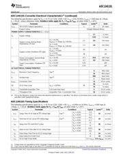
Operating Ratings
(1)(2)
Operating Temperature Range −40°C ≤ T
A
≤ +85°C
V
A
Supply Voltage +2.7V to +5.25V
Digital Input Pins Voltage Range −0.3V to V
A
Clock Frequency 50 kHz to 16 MHz
Analog Input Voltage 0V to V
A
(1) Absolute Maximum Ratings indicate limits beyond which damage to the device may occur. Operating Ratings indicate conditions for
which the device is functional, but do not ensure specific performance limits. For ensured specifications and test conditions, see the
Electrical Characteristics. The ensured specifications apply only for the test conditions listed. Some performance characteristics may
degrade when the device is not operated under the listed test conditions.
(2) All voltages are measured with respect to GND = 0V, unless otherwise specified.
Package Thermal Resistance
(1)(2)
Package θ
JA
10-lead VSSOP 190°C / W
(1) Soldering process must comply with TI's Reflow Temperature Profile specifications.
(2) Reflow temperature profiles are different for lead-free and non-lead-free packages.
Copyright © 2005–2013, Texas Instruments Incorporated Submit Documentation Feedback 3
Product Folder Links: ADC124S101
器件 Datasheet 文档搜索
AiEMA 数据库涵盖高达 72,405,303 个元件的数据手册,每天更新 5,000 多个 PDF 文件
