Datasheet 搜索 > 开发套件 > TI(德州仪器) > ADS4449EVM 数据手册 > ADS4449EVM 数据手册 2/56 页

¥ 5221.148
ADS4449EVM 数据手册 - TI(德州仪器)
制造商:
TI(德州仪器)
分类:
开发套件
Pictures:
3D模型
符号图
焊盘图
引脚图
产品图
页面导航:
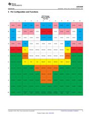
引脚图在P3P4Hot
典型应用电路图在P41P42P43P44
原理图在P21
封装尺寸在P51P53P54
标记信息在P51
封装信息在P50P51P52P53P54
技术参数、封装参数在P5
应用领域在P1P56
电气规格在P7P8
导航目录
ADS4449EVM数据手册
Page:
of 56 Go
若手册格式错乱,请下载阅览PDF原文件

2
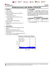
ADS4449
SBAS603A –APRIL 2013–REVISED JANUARY 2016
www.ti.com
Product Folder Links: ADS4449
Submit Documentation Feedback Copyright © 2013–2016, Texas Instruments Incorporated
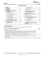
Table of Contents
1 Features.................................................................. 1
2 Applications ........................................................... 1
3 Description............................................................. 1
4 Revision History..................................................... 2
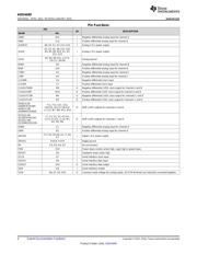
5 Pin Configuration and Functions......................... 3
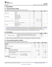
6 Specifications......................................................... 5
6.1 Absolute Maximum Ratings ...................................... 5
6.2 ESD Ratings.............................................................. 5
6.3 Recommended Operating Conditions....................... 5
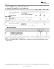
6.4 Thermal Information.................................................. 6
6.5 Electrical Characteristics........................................... 7
6.6 Digital Characteristics ............................................... 9
6.7 Timing Requirements.............................................. 10
6.8 Timing Characteristics For Figure 1........................ 10
6.9 Typical Characteristics............................................ 12
6.10 Typical Characteristics: Contour........................... 18
7 Parameter Measurement Information ................ 19
7.1 LVDS Output Timing............................................... 19
8 Detailed Description............................................ 21
8.1 Overview................................................................. 21
8.2 Functional Block Diagram....................................... 21
8.3 Feature Description................................................. 22
8.4 Device Functional Modes........................................ 23
8.5 Programming .......................................................... 26
8.6 Register Maps ........................................................ 28
9 Application and Implementation ........................ 41
9.1 Application Information............................................ 41
9.2 Typical Application.................................................. 41
10 Power Supply Recommendations ..................... 48
11 Layout................................................................... 48
11.1 Layout Guidelines ................................................. 48
11.2 Layout Example ................................................... 48
12 Device and Documentation Support................. 49
12.1 Device Nomenclature............................................ 49
12.2 Documentation Support ........................................ 50
12.3 Community Resources.......................................... 50
12.4 Trademarks........................................................... 50
12.5 Electrostatic Discharge Caution............................ 50
12.6 Glossary................................................................ 50
13 Mechanical, Packaging, and Orderable
Information........................................................... 50
4 Revision History
NOTE: Page numbers for previous revisions may differ from page numbers in the current version.
Changes from Original (April 2013) to Revision A Page
• Added Internal Dither Features bullet .................................................................................................................................... 1
• Added ESD Ratings table, Feature Description section, Device Functional Modes section, Application and
Implementation section, Power Supply Recommendations section, Layout section, Device and Documentation
Support section, and Mechanical, Packaging, and Orderable Information section................................................................ 1
• Deleted Package and Ordering Information because the data is repeated in the Package Option Addendum ................... 1
• Deleted SNRB from the configuration registers block in the functional block diagram ......................................................... 1
• Changed Clock Inputs, Input clock sample rate parameter minimum specification in Recommended Operating
Conditions table...................................................................................................................................................................... 5
• Changed Table 2 ................................................................................................................................................................. 22
器件 Datasheet 文档搜索
AiEMA 数据库涵盖高达 72,405,303 个元件的数据手册,每天更新 5,000 多个 PDF 文件
