Datasheet 搜索 > 开发套件 > TI(德州仪器) > ADS4449EVM 数据手册 > ADS4449EVM 数据手册 4/56 页

¥ 5221.148
ADS4449EVM 数据手册 - TI(德州仪器)
制造商:
TI(德州仪器)
分类:
开发套件
Pictures:
3D模型
符号图
焊盘图
引脚图
产品图
页面导航:
引脚图在P3P4Hot
典型应用电路图在P41P42P43P44
原理图在P21
封装尺寸在P51P53P54
标记信息在P51
封装信息在P50P51P52P53P54
技术参数、封装参数在P5
应用领域在P1P56
电气规格在P7P8
导航目录
ADS4449EVM数据手册
Page:
of 56 Go
若手册格式错乱,请下载阅览PDF原文件
4
ADS4449
SBAS603A –APRIL 2013–REVISED JANUARY 2016
www.ti.com
Product Folder Links: ADS4449
Submit Documentation Feedback Copyright © 2013–2016, Texas Instruments Incorporated
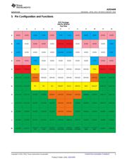
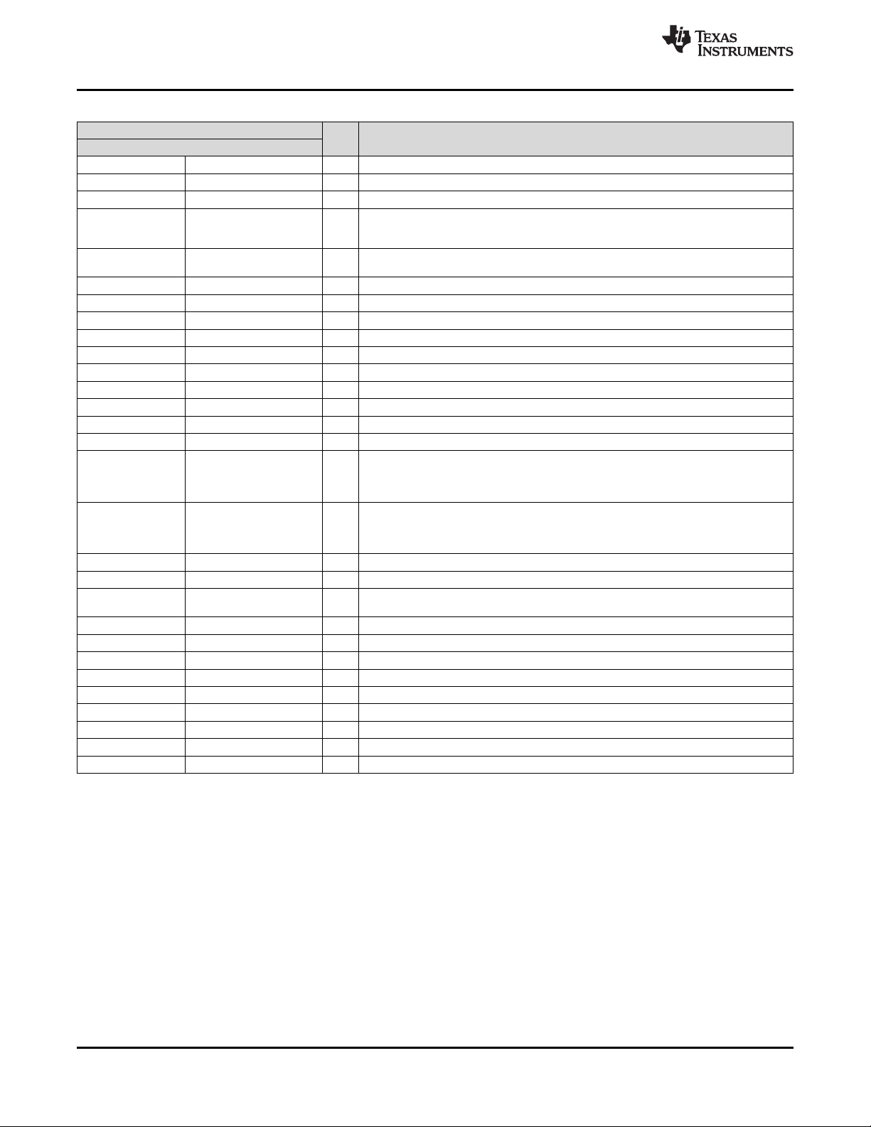
Pin Functions
PIN
I/O DESCRIPTION
NAME NO.
AINM B12 I Negative differential analog input for channel A
AINP C12 I Positive differential analog input for channel A
AVDD33 B6, B7, E1, E2, E11, E12 I Analog 3.3-V power supply
AVDD
A1, A2, A5, A8, A11, A12,
B3, B4, B9, B10, D1, D2,
D11, D12
I Analog 1.9-V power supply
AVSS
B2, B5, B8, B11, C2-C5,
C8-C11, D4-D9
I Analog ground
BINM A9 I Negative differential analog input for channel B
BINP A10 I Positive differential analog input for channel B
CINM A3 I Negative differential analog input for channel C
CINP A4 I Positive differential analog input for channel C
CLKINM C6 I Negative differential clock input
CLKINP C7 I Positive differential clock input
CLKOUTABM M9 O Negative differential LVDS clock output for channel A and B
CLKOUTABP M10 O Positive differential LVDS clock output for channel A and B
CLKOUTCDM M4 O Negative differential LVDS clock output for channels C and D
CLKOUTCDP M3 O Positive differential LVDS clock output for channels C and D
DAB[13:1]P,
DAB0P/OVRABP,
DAB[13:1]M,
DAB0M/OVRABM
F11, F12, G11, G12,
H9-H12, J8-J12, K8-K12,
L7-L12, M7, M8, M11, M12
O DDR LVDS outputs for channels A and B.
DCD[13:1]P,
DCD0P/OVRCDP,
DCD[13:1]M,
DCD0M/OVRCDM
F1, F2, G1, G2, H1-H4,
J1-J5, K1-K5, L1-L6, M1,
M2, M5, M6
O DDR LVDS outputs for channels C and D.
DINM C1 I Negative differential analog input for channel D
DINP B1 I Positive differential analog input for channel D
DRVDD
F3, F10, H5-H8, J6, J7, K6,
K7
I Digital 1.8-V power supply
DRVSS E4-E9, F4-F9 I Digital ground
NC E3, G3, G4, G5 - Do not connect
PDN E10 I Power-down control; active high. Logic high is power down.
RESET G6 I Hardware reset; active high
SCLK G7 I Serial interface clock input
SDATA G8 I Serial interface data input
SDOUT G10 O Serial interface data output
SEN G9 I Serial interface enable
VCM A6, A7, D3, D10 O Common-mode voltage for analog inputs. All VCM terminals are internally connected together.
器件 Datasheet 文档搜索
AiEMA 数据库涵盖高达 72,405,303 个元件的数据手册,每天更新 5,000 多个 PDF 文件
