Datasheet 搜索 > 开发套件 > TI(德州仪器) > ADS4449EVM 数据手册 > ADS4449EVM 数据手册 5/56 页

¥ 5221.148
ADS4449EVM 数据手册 - TI(德州仪器)
制造商:
TI(德州仪器)
分类:
开发套件
Pictures:
3D模型
符号图
焊盘图
引脚图
产品图
页面导航:
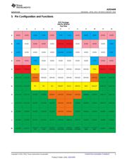
引脚图在P3P4Hot
典型应用电路图在P41P42P43P44
原理图在P21
封装尺寸在P51P53P54
标记信息在P51
封装信息在P50P51P52P53P54
技术参数、封装参数在P5
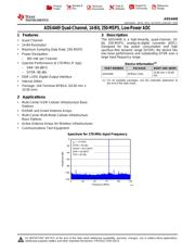
应用领域在P1P56
电气规格在P7P8
导航目录
ADS4449EVM数据手册
Page:
of 56 Go
若手册格式错乱,请下载阅览PDF原文件
5
ADS4449
www.ti.com
SBAS603A –APRIL 2013–REVISED JANUARY 2016
Product Folder Links: ADS4449
Submit Documentation FeedbackCopyright © 2013–2016, Texas Instruments Incorporated
(1) Stresses beyond those listed under Absolute Maximum Ratings may cause permanent damage to the device. These are stress ratings
only, which do not imply functional operation of the device at these or any other conditions beyond those indicated under Recommended
Operating Conditions. Exposure to absolute-maximum-rated conditions for extended periods may affect device reliability.
(2) When AVDD is turned off, TI recommends switching off the input clock (or ensuring the voltage on CLKP and CLKM is less than
| 0.3 V |). This recommendation prevents the ESD protection diodes at the clock input terminals from turning on.
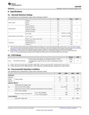
6 Specifications
6.1 Absolute Maximum Ratings
over operating free-air temperature range (unless otherwise noted)
(1)
MIN MAX UNIT
Supply voltage
AVDD33 –0.3 3.6
VAVDD –0.3 2.1
DRVDD –0.3 2.1
Voltage between
AVSS and DRVSS –0.3 0.3
V
AVDD and DRVDD –2.4 2.4
AVDD33 and DRVDD –2.4 3.9
AVDD33 and AVDD –2.4 3.9
Voltage applied to input terminals
XINP, XINM –0.3
minimum (1.9, AVDD +
0.3)
V
CLKP, CLKM
(2)
–0.3
minimum (1.9, AVDD +
0.3)
RESET, SCLK, SDATA, SEN, PDN –0.3 3.9
Temperature
Operating free-air, T
A
–40 85
°COperating junction, T
J
150
Storage, T
stg
–65 150
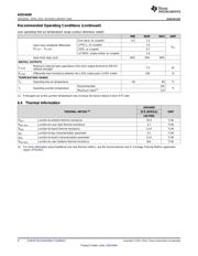
(1) JEDEC document JEP155 states that 500-V HBM allows safe manufacturing with a standard ESD control process.
(2) JEDEC document JEP157 states that 250-V CDM allows safe manufacturing with a standard ESD control process.
6.2 ESD Ratings
VALUE UNIT
V
(ESD)
Electrostatic discharge
Human-body model (HBM), per ANSI/ESDA/JEDEC JS-001
(1)
±2000
V
Charged-device model (CDM), per JEDEC specification JESD22-
C101
(2)
±500
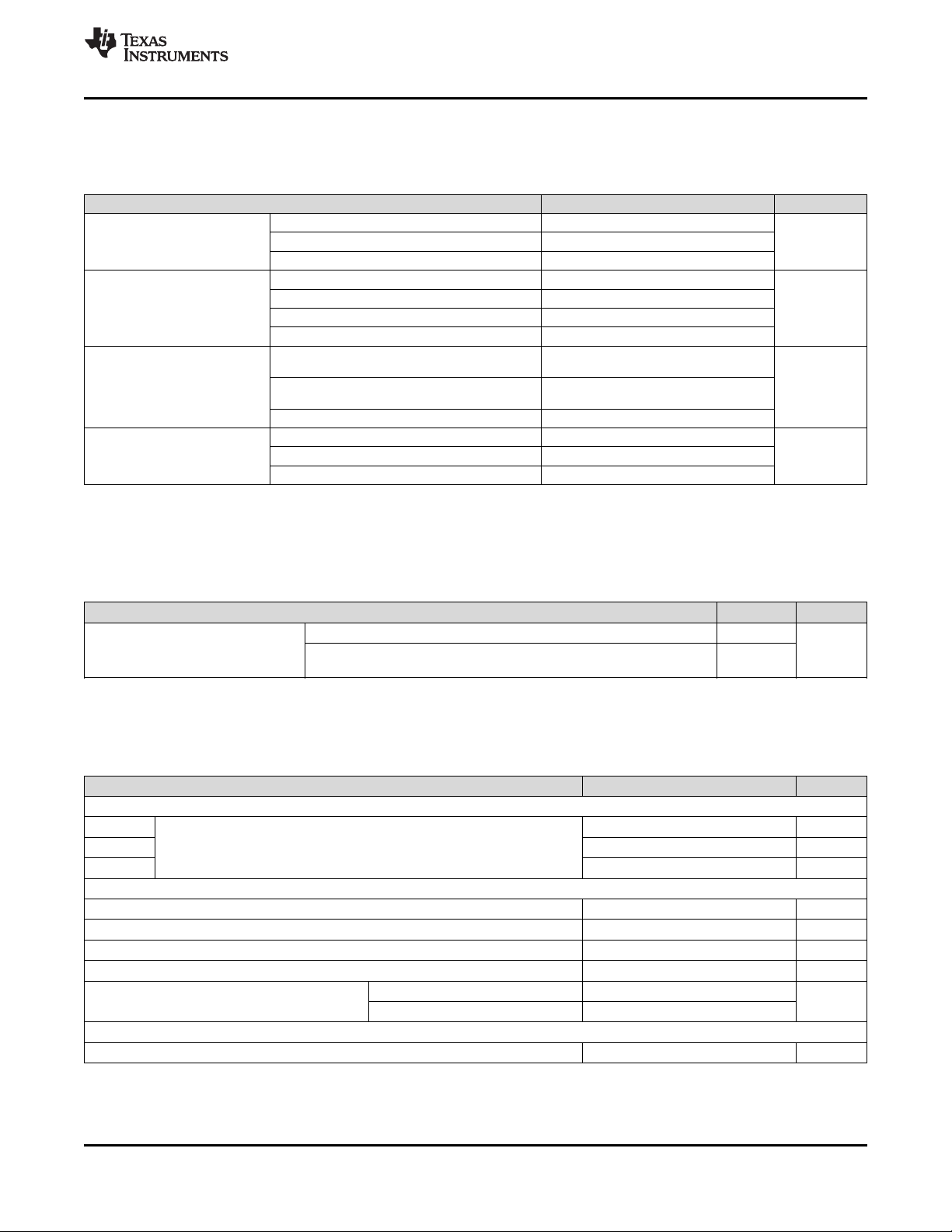
6.3 Recommended Operating Conditions
over operating free-air temperature range (unless otherwise noted)
MIN NOM MAX UNIT
SUPPLIES
AVDD33
Supply voltage
3.15 3.3 3.45 V
AVDD 1.8 1.9 2 V
DRVDD 1.7 1.8 2 V
ANALOG INPUTS
Differential input voltage range 2 V
PP
V
IC
Input common-mode voltage V
CM
± 0.025 V
Analog input common-mode current (per input terminal of each channel) 1.5 µA/MSPS
VCM current capability 5 mA
Maximum analog input frequency
2-V
PP
input amplitude 400
MHz
1.4-V
PP
input amplitude 500
CLOCK INPUTS
Input clock sample rate 10 250 MSPS
器件 Datasheet 文档搜索
AiEMA 数据库涵盖高达 72,405,303 个元件的数据手册,每天更新 5,000 多个 PDF 文件
