Datasheet 搜索 > RF射频器件 > TI(德州仪器) > CC1101RGPR 数据手册 > CC1101RGPR 数据手册 31/105 页
 器件3D模型
¥ 3.928
CC1101RGPR 数据手册 - TI(德州仪器)
制造商:
TI(德州仪器)
分类:
RF射频器件
封装:
QFN-20
描述:
TEXAS INSTRUMENTS CC1101RGPR 芯片, 射频收发器, QFN-20
Pictures:
3D模型
符号图
焊盘图
引脚图
产品图
页面导航:
引脚图在P20P34P71Hot
典型应用电路图在P25
原理图在P22
封装尺寸在P99
焊盘布局在P26
型号编码规则在P95
标记信息在P99
封装信息在P99P100
焊接温度在P8
功能描述在P2
技术参数、封装参数在P8P9P34
应用领域在P1P105
电气规格在P9
导航目录
CC1101RGPR数据手册
Page:
of 105 Go
若手册格式错乱,请下载阅览PDF原文件
CC1101
SWRS061I Page 31 of 98
10.1 Chip Status Byte
When the header byte, data byte, or command
strobe is sent on the SPI interface, the chip
status byte is sent by the
CC1101
on the SO pin.
The status byte contains key status signals,
useful for the MCU. The first bit, s7, is the
CHIP_RDYn signal and this signal must go low
before the first positive edge of SCLK. The
CHIP_RDYn signal indicates that the crystal is
running.
Bits 6, 5, and 4 comprise the STATE value.
This value reflects the state of the chip. The
XOSC and power to the digital core are on in
the IDLE state, but all other modules are in
power down. The frequency and channel
configuration should only be updated when the
chip is in this state. The RX state will be active
when the chip is in receive mode. Likewise, TX
is active when the chip is transmitting.
The last four bits (3:0) in the status byte
contains FIFO_BYTES_AVAILABLE. For read
operations (the R/W¯ bit in the header byte is
set to 1), the FIFO_BYTES_AVAILABLE field
contains the number of bytes available for
reading from the RX FIFO. For write
operations (the R/W¯ bit in the header byte is
set to 0), the FIFO_BYTES_AVAILABLE field
contains the number of bytes that can be
written to the TX FIFO. When
FIFO_BYTES_AVAILABLE=15, 15 or more
bytes are available/free.
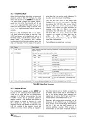
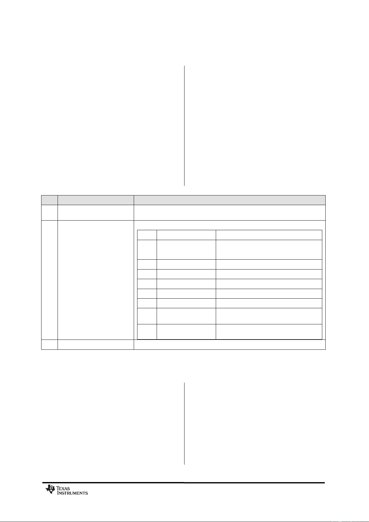
Table 23 gives a status byte summary.
Bits
Name
Description
7
CHIP_RDYn
Stays high until power and crystal have stabilized. Should always be low when using
the SPI interface.
6:4
STATE[2:0]
Indicates the current main state machine mode
Value
State
Description
000
IDLE
IDLE state
(Also reported for some transitional states instead
of SETTLING or CALIBRATE)
001
RX
Receive mode
010
TX
Transmit mode
011
FSTXON
Fast TX ready
100
CALIBRATE
Frequency synthesizer calibration is running
101
SETTLING
PLL is settling
110
RXFIFO_OVERFLOW
RX FIFO has overflowed. Read out any
useful data, then flush the FIFO with SFRX
111
TXFIFO_UNDERFLOW
TX FIFO has underflowed. Acknowledge with
SFTX
3:0
FIFO_BYTES_AVAILABLE[3:0]
The number of bytes available in the RX FIFO or free bytes in the TX FIFO
Table 23: Status Byte Summary
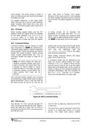
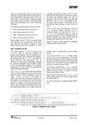
10.2 Register Access
The configuration registers on the
CC1101
are
located on SPI addresses from 0x00 to 0x2E.
Table 43 on page 68 lists all configuration
registers. It is highly recommended to use
SmartRF Studio [5] to generate optimum
register settings. The detailed description of
each register is found in Section 29.1 and
29.2, starting on page 71. All configuration
registers can be both written to and read. The
R/W¯ bit controls if the register should be
written to or read. When writing to registers,
the status byte is sent on the SO pin each time
a header byte or data byte is transmitted on
the SI pin. When reading from registers, the
status byte is sent on the SO pin each time a
header byte is transmitted on the SI pin.
Registers with consecutive addresses can be
accessed in an efficient way by setting the
burst bit (B) in the header byte. The address
bits (A
5
– A
0
) set the start address in an
internal address counter. This counter is
incremented by one each new byte (every 8
器件 Datasheet 文档搜索
AiEMA 数据库涵盖高达 72,405,303 个元件的数据手册,每天更新 5,000 多个 PDF 文件
