Datasheet 搜索 > RF射频器件 > TI(德州仪器) > CC1101RGPR 数据手册 > CC1101RGPR 数据手册 34/105 页
 器件3D模型
¥ 3.93
CC1101RGPR 数据手册 - TI(德州仪器)
制造商:
TI(德州仪器)
分类:
RF射频器件
封装:
QFN-20
描述:
TEXAS INSTRUMENTS CC1101RGPR 芯片, 射频收发器, QFN-20
Pictures:
3D模型
符号图
焊盘图
引脚图
产品图
页面导航:
引脚图在P20P34P71Hot
典型应用电路图在P25
原理图在P22
封装尺寸在P99
焊盘布局在P26
型号编码规则在P95
标记信息在P99
封装信息在P99P100
焊接温度在P8
功能描述在P2
技术参数、封装参数在P8P9P34
应用领域在P1P105
电气规格在P9
导航目录
CC1101RGPR数据手册
Page:
of 105 Go
若手册格式错乱,请下载阅览PDF原文件
CC1101
SWRS061I Page 34 of 98
11 Microcontroller Interface and Pin Configuration
In a typical system,
CC1101
will interface to a
microcontroller. This microcontroller must be
able to:
Program
CC1101
into different modes
Read and write buffered data
Read back status information via the 4-wire
SPI-bus configuration interface (SI, SO,
SCLK and CSn)
11.1 Configuration Interface
The microcontroller uses four I/O pins for the
SPI configuration interface (SI, SO, SCLK and
CSn). The SPI is described in Section 10 on
page 29.
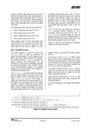
11.2 General Control and Status Pins
The
CC1101
has two dedicated configurable
pins (GDO0 and GDO2) and one shared pin
(GDO1) that can output internal status
information useful for control software. These
pins can be used to generate interrupts on the
MCU. See Section 26 on page 61 for more
details on the signals that can be
programmed.
GDO1 is shared with the SO pin in the SPI
interface. The default setting for GDO1/SO is
3-state output. By selecting any other of the
programming options, the GDO1/SO pin will
become a generic pin. When CSn is low, the
pin will always function as a normal SO pin.
In the synchronous and asynchronous serial
modes, the GDO0 pin is used as a serial TX
data input pin while in transmit mode.
The GDO0 pin can also be used for an on-chip
analog temperature sensor. By measuring the
voltage on the GDO0 pin with an external
ADC, the temperature can be calculated.
Specifications for the temperature sensor are
found in Section 4.7. With default PTEST
register setting (0x7F), the temperature sensor
output is only available if the frequency
synthesizer is enabled (e.g. the MANCAL,
FSTXON, RX, and TX states). It is necessary
to write 0xBF to the PTEST register to use the
analog temperature sensor in the IDLE state.
Before leaving the IDLE state, the PTEST
register should be restored to its default value
(0x7F).
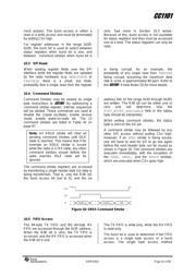
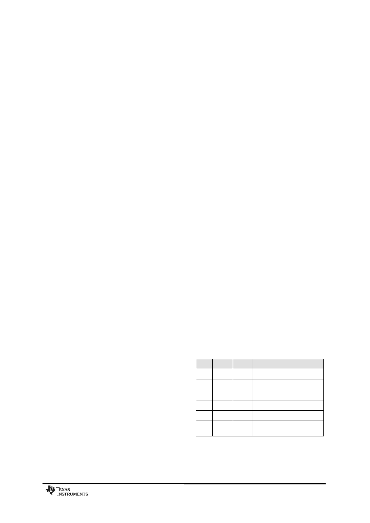
11.3 Optional Radio Control Feature
The
CC1101
has an optional way of controlling
the radio by reusing SI, SCLK, and CSn from
the SPI interface. This feature allows for a
simple three-pin control of the major states of
the radio: SLEEP, IDLE, RX, and TX. This
optional functionality is enabled with the
MCSM0.PIN_CTRL_EN configuration bit.
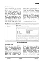
State changes are commanded as follows:
If CSn is high, the SI and SCLK are set to
the desired state according to Table 24.
If CSn goes low, the state of SI and SCLK
is latched and a command strobe is
generated internally according to the pin
configuration.
It is only possible to change state with the
latter functionality. That means that for
instance RX will not be restarted if SI and
SCLK are set to RX and CSn toggles. When
CSn is low the SI and SCLK has normal SPI
functionality.
All pin control command strobes are executed
immediately except the SPWD strobe. The
SPWD strobe is delayed until CSn goes high.
CSn
SCLK
SI
Function
1
X
X
Chip unaffected by SCLK/SI
0
0
Generates SPWD strobe
0
1
Generates STX strobe
1
0
Generates SIDLE strobe
1
1
Generates SRX strobe
0
SPI
mode
SPI
mode
SPI mode (wakes up into
IDLE if in SLEEP/XOFF)
Table 24: Optional Pin Control Coding
器件 Datasheet 文档搜索
AiEMA 数据库涵盖高达 72,405,303 个元件的数据手册,每天更新 5,000 多个 PDF 文件
