Datasheet 搜索 > RF射频器件 > TI(德州仪器) > CC1101RGPR 数据手册 > CC1101RGPR 数据手册 33/105 页
 器件3D模型
¥ 3.928
CC1101RGPR 数据手册 - TI(德州仪器)
制造商:
TI(德州仪器)
分类:
RF射频器件
封装:
QFN-20
描述:
TEXAS INSTRUMENTS CC1101RGPR 芯片, 射频收发器, QFN-20
Pictures:
3D模型
符号图
焊盘图
引脚图
产品图
页面导航:
引脚图在P20P34P71Hot
典型应用电路图在P25
原理图在P22
封装尺寸在P99
焊盘布局在P26
型号编码规则在P95
标记信息在P99
封装信息在P99P100
焊接温度在P8
功能描述在P2
技术参数、封装参数在P8P9P34
应用领域在P1P105
电气规格在P9
导航目录
CC1101RGPR数据手册
Page:
of 105 Go
若手册格式错乱,请下载阅览PDF原文件
CC1101
SWRS061I Page 33 of 98
expects a header byte with the burst bit set to
zero and one data byte. After the data byte, a
new header byte is expected; hence, CSn can
remain low. The burst access method expects
one header byte and then consecutive data
bytes until terminating the access by setting
CSn high.
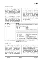
The following header bytes access the FIFOs:
0x3F: Single byte access to TX FIFO
0x7F: Burst access to TX FIFO
0xBF: Single byte access to RX FIFO
0xFF: Burst access to RX FIFO
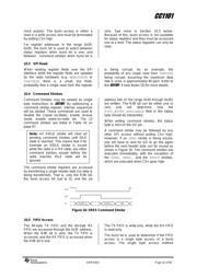
When writing to the TX FIFO, the status byte
(see Section 10.1) is output on SO for each
new data byte as shown in Figure 15. This
status byte can be used to detect TX FIFO
underflow while writing data to the TX FIFO.
Note that the status byte contains the number
of bytes free before writing the byte in
progress to the TX FIFO. When the last byte
that fits in the TX FIFO is transmitted on SI,
the status byte received concurrently on SO
will indicate that one byte is free in the TX
FIFO.
The TX FIFO may be flushed by issuing a
SFTX command strobe. Similarly, a SFRX
command strobe will flush the RX FIFO. A
SFTX or SFRX command strobe can only be
issued in the IDLE, TXFIFO_UNDERFLOW, or
RXFIFO_OVERFLOW states. Both FIFOs are
flushed when going to the SLEEP state.
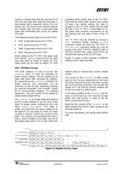
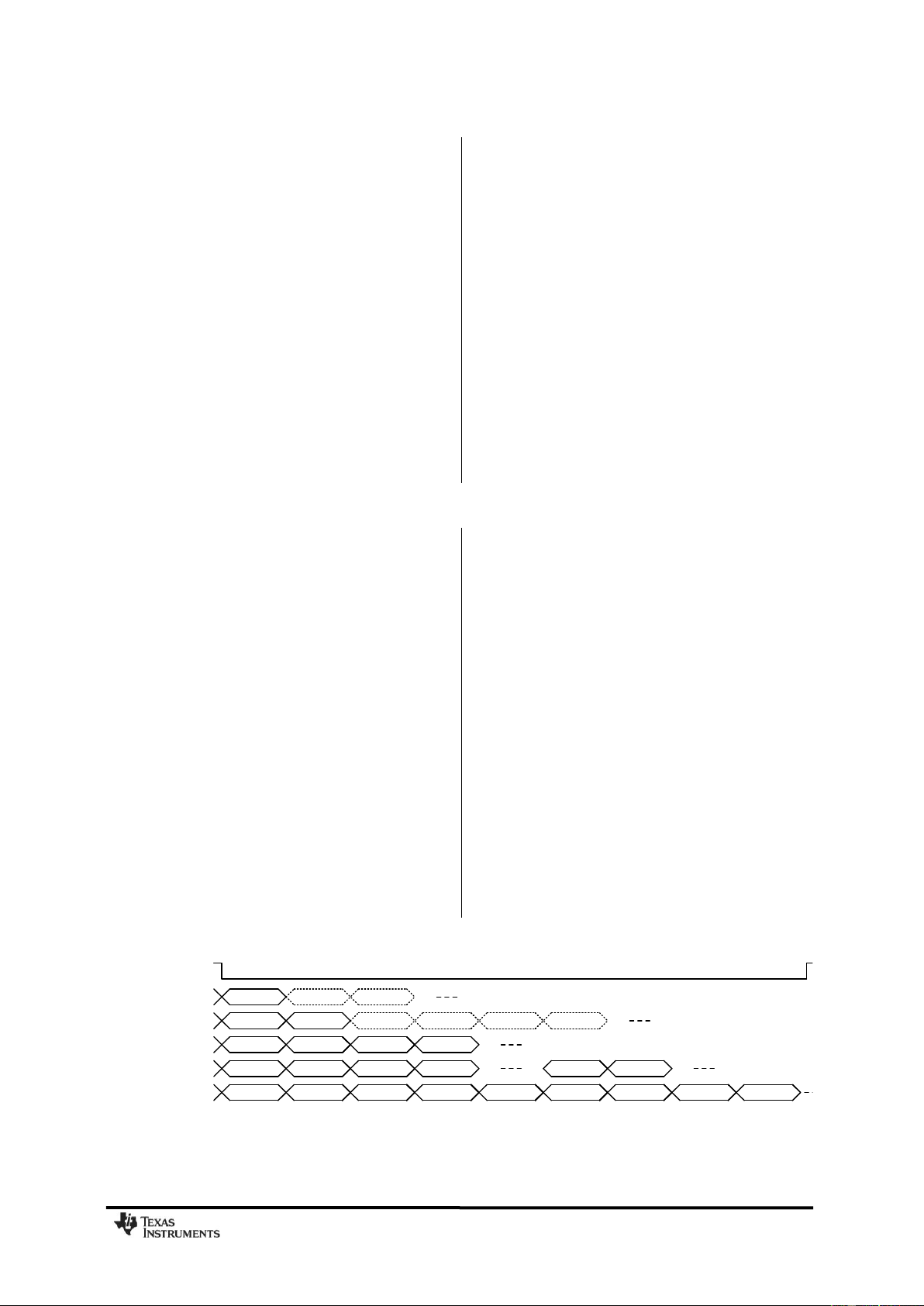
Figure 17 gives a brief overview of different
register access types possible.
10.6 PATABLE Access
The 0x3E address is used to access the
PATABLE, which is used for selecting PA
power control settings. The SPI expects up to
eight data bytes after receiving the address.
By programming the PATABLE, controlled PA
power ramp-up and ramp-down can be
achieved, as well as ASK modulation shaping
for reduced bandwidth. See SmartRF Studio
[5] for recommended shaping / PA ramping
sequences. See also Section 24 for details on
output power programming.
The PATABLE is an 8-byte table that defines
the PA control settings to use for each of the
eight PA power values (selected by the 3-bit
value FREND0.PA_POWER). The table is
written and read from the lowest setting (0) to
the highest (7), one byte at a time. An index
counter is used to control the access to the
table. This counter is incremented each time a
byte is read or written to the table, and set to
the lowest index when CSn is high. When the
highest value is reached the counter restarts
at zero.
The access to the PATABLE is either single
byte or burst access depending on the burst
bit. When using burst access the index counter
will count up; when reaching 7 the counter will
restart at 0. The R/W¯ bit controls whether the
access is a read or a write access.
If one byte is written to the PATABLE and this
value is to be read out, CSn must be set high
before the read access in order to set the
index counter back to zero.
Note that the content of the PATABLE is lost
when entering the SLEEP state, except for the
first byte (index 0).
For more information, see Design Note DN501
[18].
Read or write consecutive
Read or write n + 1 bytes
registers (burst):
from/to the RX/TX FIFO:
Header
Strobe
Header
Strobe
Header
Strobe
Header
Reg
Header
Reg n
Header
FIFO
Header
Reg
Data
Data
n
Data
Byte 0
Data
Header
Reg
Data Header
Reg
Data
Data
n + 1
Data
n + 2
Header
Strobe
Header
Reg
Data Header
Strobe
Header
FIFO
Data
Byte 1
Data
Byte 2
Data
Byte n - 1
Data
Byte n
Data
Byte 0
Data
Byte 1
CSn:
Command strobe(s):
Read or write register(s):
Combinations:
Figure 17: Register Access Types
器件 Datasheet 文档搜索
AiEMA 数据库涵盖高达 72,405,303 个元件的数据手册,每天更新 5,000 多个 PDF 文件
