Datasheet 搜索 > MOS管 > TI(德州仪器) > CSD19537Q3 数据手册 > CSD19537Q3 数据手册 3/13 页

¥ 2.542
CSD19537Q3 数据手册 - TI(德州仪器)
制造商:
TI(德州仪器)
分类:
MOS管
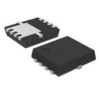
封装:
VSON-Clip-8
描述:
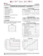
CSD19537Q3,100V N 沟道 NexFET(TM) 功率 MOSFET
Pictures:
3D模型
符号图
焊盘图
引脚图
产品图
页面导航:
导航目录
CSD19537Q3数据手册
Page:
of 13 Go
若手册格式错乱,请下载阅览PDF原文件
CSD19537Q3
www.ti.com
SLPS549 –AUGUST 2015
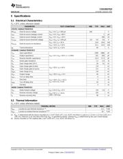
5 Specifications
5.1 Electrical Characteristics
(T
A
= 25°C unless otherwise stated)
PARAMETER TEST CONDITIONS MIN TYP MAX UNIT
STATIC CHARACTERISTICS
BV
DSS
Drain-to-source voltage V
GS
= 0 V, I
D
= 250 μA 100 V
I
DSS
Drain-to-source leakage current V
GS
= 0 V, V
DS
= 80 V 1 μA
I
GSS
Gate-to-source leakage current V
DS
= 0 V, V
GS
= 20 V 100 nA
V
GS(th)
Gate-to-source threshold voltage V
DS
= V
GS
, I
D
= 250 μA 2.6 3.0 3.6 V
V
GS
= 6 V, I
D
= 10 A 13.8 16.6 mΩ
R
DS(on)
Drain-to-source on-resistance
V
GS
= 10 V, I
D
= 10 A 12.1 14.5 mΩ
g
fs
Transconductance V
DS
= 10 V, I
D
= 10 A 45 S
DYNAMIC CHARACTERISTICS
C
iss
Input capacitance 1290 1680 pF
C
oss
Output capacitance V
GS
= 0 V, V
DS
= 50 V, ƒ = 1 MHz 251 326 pF
C
rss
Reverse transfer capacitance 13.3 17.3 pF
R
G
Series gate resistance 1.2 2.4 Ω
Q
g
Gate charge total (10 V) 16 21 nC
Q
gd
Gate charge gate to drain 2.9 nC
V
DS
= 50 V, I
D
= 10 A
Q
gs
Gate charge gate to source 5.5 nC
Q
g(th)
Gate charge at V
th
3.8 nC
Q
oss
Output charge V
DS
= 50 V, V
GS
= 0 V 44 nC
t
d(on)
Turn on delay time 5 ns
t
r
Rise time 3 ns
V
DS
= 50 V, V
GS
= 10 V,
I
DS
= 10 A, R
G
= 0 Ω
t
d(off)
Turn off delay time 10 ns
t
f
Fall time 3 ns
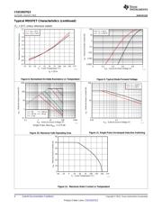
DIODE CHARACTERISTICS
V
SD
Diode forward voltage I
SD
= 10 A, V
GS
= 0 V 0.8 1.0 V
Q
rr
Reverse recovery charge 134 nC
V
DS
= 50 V, I
F
= 10 A,
di/dt = 300 A/μs
t
rr
Reverse recovery time 36 ns
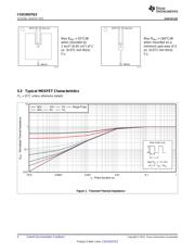
5.2 Thermal Information
(T
A
= 25°C unless otherwise stated)
THERMAL METRIC MIN TYP MAX UNIT
R
θJC
Junction-to-case thermal resistance
(1)
1.5 °C/W
R
θJA
Junction-to-ambient thermal resistance
(1)(2)
55 °C/W
(1) R
θJC
is determined with the device mounted on a 1 inch
2
(6.45 cm
2
), 2 oz. (0.071 mm thick) Cu pad on a 1.5 inch × 1.5 inch (3.81 cm ×
3.81 cm), 0.06 inch (1.52 mm) thick FR4 PCB. R
θJC
is specified by design, whereas R
θJA
is determined by the user’s board design.
(2) Device mounted on FR4 material with 1 inch
2
(6.45 cm
2
), 2 oz. (0.071 mm thick) Cu.
Copyright © 2015, Texas Instruments Incorporated Submit Documentation Feedback 3
Product Folder Links: CSD19537Q3
器件 Datasheet 文档搜索
AiEMA 数据库涵盖高达 72,405,303 个元件的数据手册,每天更新 5,000 多个 PDF 文件
