Datasheet 搜索 > Infineon(英飞凌) > IRF3808S 数据手册 > IRF3808S 数据手册 2/12 页


¥ 0
IRF3808S 数据手册 - Infineon(英飞凌)
制造商:
Infineon(英飞凌)
封装:
TO-263
Pictures:
3D模型
符号图
焊盘图
引脚图
产品图
页面导航:
导航目录
IRF3808S数据手册
Page:
of 12 Go
若手册格式错乱,请下载阅览PDF原文件
AUIRF3808S
2 2015-11-13
Notes:
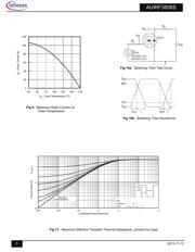
Repetitive rating; pulse width limited by max. junction temperature. (See fig.11)
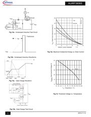
Starting T
J
= 25°C, L = 0.130mH, R
G
= 25, I
AS
= 82A. (See fig.12)
I
SD
82A, di/dt 310A/µs, V
DD
V
(BR)DSS
, T
J
175°C.
Pulse width 400µs; duty cycle 2%.
C
oss eff.
is a fixed capacitance that gives the same charging time as C
oss
while V
DS
is rising from 0 to 80% V
DSS
.
Limited by T
Jmax
, see Fig.12a, 12b, 15, 16 for typical repetitive avalanche performance.
When mounted on 1" square PCB (FR-4 or G-10 Material). For recommended footprint and soldering techniques refer to application
note #AN-994
R
is measured at T
J
of approximately 90°C
Static @ T
J
= 25°C (unless otherwise specified)
Parameter Min. Typ. Max. Units Conditions
V
(BR)DSS
Drain-to-Source Breakdown Voltage 75 ––– ––– V V
GS
= 0V, I
D
= 250µA
V
(BR)DSS
/T
J
Breakdown Voltage Temp. Coefficient ––– 0.086 ––– V/°C Reference to 25°C, I
D
= 1mA
R
DS(on)
Static Drain-to-Source On-Resistance ––– 5.9 7.0
m
V
GS
= 10V, I
D
= 82A
V
GS(th)
Gate Threshold Voltage 2.0 ––– 4.0 V V
DS
= V
GS
, I
D
= 250µA
g
fs
Forward Transconductance 100 ––– ––– S V
DS
= 25V, I
D
= 82A
I
DSS
Drain-to-Source Leakage Current
––– ––– 25
µA
V
DS
= 75V, V
GS
= 0V
––– ––– 250 V
DS
= 60V,V
GS
= 0V,T
J
=150°C
I
GSS
Gate-to-Source Forward Leakage ––– ––– 200
nA
V
GS
= 20V
Gate-to-Source Reverse Leakage ––– ––– -200 V
GS
= -20V
Dynamic Electrical Characteristics @ T
J
= 25°C (unless otherwise specified)
Q
g
Total Gate Charge ––– 150 220
nC
I
D
= 82A
Q
gs
Gate-to-Source Charge ––– 31 47
V
DS
= 60V
Q
gd
Gate-to-Drain Charge ––– 50 76
V
GS
= 10V
t
d(on)
Turn-On Delay Time ––– 16 –––
ns
V
DD
= 38V
t
r
Rise Time ––– 140 ––– I
D
= 82A
t
d(off)
Turn-Off Delay Time ––– 68 –––
R
G
= 2.5
t
f
Fall Time ––– 120 –––
V
GS
= 10V
L
D
Internal Drain Inductance ––– 4.5 –––
nH
Between lead,
6mm (0.25in.)
L
S
Internal Source Inductance ––– 7.5 –––
from package
and center of die contact
C
iss
Input Capacitance ––– 5310 –––
pF
V
GS
= 0V
C
oss
Output Capacitance ––– 890 ––– V
DS
= 25V
C
rss
Reverse Transfer Capacitance ––– 130 –––
ƒ = 1.0MHz, See Fig.5
C
oss
Output Capacitance ––– 6010 ––– V
GS
= 0V,V
DS
= 1.0V, ƒ = 1.0MHz
C
oss
Output Capacitance ––– 570 ––– V
GS
= 0V,V
DS
= 60V, ƒ = 1.0MHz
C
oss eff.
Effective Output Capacitance (Time Related) ––– 1140 ––– V
GS
= 0V,V
DS
= 0V to 60V
Diode Characteristics
Parameter Min. Typ. Max. Units Conditions
I
S
Continuous Source Current
––– ––– 106
A
MOSFET symbol
(Body Diode)
showing the
I
SM
Pulsed Source Current
––– ––– 550
integral reverse
(Body Diode) p-n junction diode.
V
SD
Diode Forward Voltage ––– ––– 1.3 V T
J
= 25°C,I
S
= 82A,V
GS
= 0V
t
rr
Reverse Recovery Time ––– 93 140 ns
T
J
= 25°C ,I
F
= 82A
Q
rr
Reverse Recovery Charge ––– 340 510 nC
di/dt = 100A/µs
t
on
Forward Turn-On Time
Intrinsic turn-on time is negligible (turn-on is dominated by L
S
+L
D
)
器件 Datasheet 文档搜索
AiEMA 数据库涵盖高达 72,405,303 个元件的数据手册,每天更新 5,000 多个 PDF 文件
