Datasheet 搜索 > MOS管 > Infineon(英飞凌) > IRF40H210 数据手册 > IRF40H210 数据手册 2/11 页
 器件3D模型
¥ 7.634
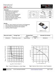
IRF40H210 数据手册 - Infineon(英飞凌)
制造商:
Infineon(英飞凌)
分类:
MOS管
封装:
PQFN-8
描述:
IRF40H210 编带
Pictures:
3D模型
符号图
焊盘图
引脚图
产品图
页面导航:
封装尺寸在P9
标记信息在P9
封装信息在P1P10
电气规格在P3
导航目录
IRF40H210数据手册
Page:
of 11 Go
若手册格式错乱,请下载阅览PDF原文件
IRF40H210
2
www.irf.com © 2015 International Rectifier
Submit Datasheet Feedback April 1, 2015
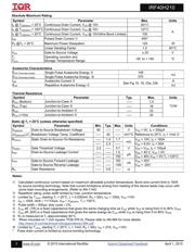
Absolute Maximum Rating
Symbol Parameter Max. Units
I
D
@ T
C(Bottom)
= 25°C Continuous Drain Current, V
GS
@ 10V 201
A
I
D
@ T
C(Bottom)
= 100°C Continuous Drain Current, V
GS
@ 10V 127
I
D
@ T
C(Bottom)
= 25°C Continuous Drain Current, V
GS
@ 10V(Wire Bond Limited) 100
I
DM
Pulsed Drain Current 400*
P
D
@T
C
= 25°C Maximum Power Dissipation 125 W
Linear Derating Factor 1.0 W/°C
V
GS
Gate-to-Source Voltage ± 20 V
T
J
T
STG
Operating Junction and
Storage Temperature Range
-55 to + 150 °C
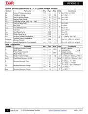
Static @ T
J
= 25°C (unless otherwise specified)
Symbol Parameter Min. Typ. Max. Units Conditions
V
(BR)DSS
Drain-to-Source Breakdown Voltage 40 ––– ––– V V
GS
= 0V, I
D
= 250µA
V
(BR)DSS
/T
J
Breakdown Voltage Temp. Coefficient ––– 42 ––– mV/°C Reference to 25°C, I
D
= 1mA
R
DS(on)
Static Drain-to-Source On-Resistance ––– 1.4 1.7 V
GS
= 10V, I
D
= 100A
––– 2.3 ––– V
GS
= 6.0V, I
D
= 50A
V
GS(th)
Gate Threshold Voltage 2.2 ––– 3.7 V V
DS
= V
GS
, I
D
= 150µA
I
DSS
Drain-to-Source Leakage Current ––– ––– 1.0
µA
V
DS
= 40 V, V
GS
= 0V
––– ––– 150 V
DS
= 40V,V
GS
= 0V,T
J
=125°C
I
GSS
Gate-to-Source Forward Leakage ––– ––– 100
nA
V
GS
= 20V
Gate-to-Source Reverse Leakage ––– ––– -100 V
GS
= -20V
R
G
Gate Resistance ––– 2.6 –––
m
Notes:
Calculated continuous current based on maximum allowable junction temperature. Bond wire current limit is 100A
by source bonding technology. Note that current limitations arising from heating of the device leads may occur with
some lead mounting arrangements. (Refer to AN-1140)
Repetitive rating; pulse width limited by max. junction temperature.
Limited by T
Jmax
, starting T
J
= 25°C, L = 0.030mH, R
G
= 50, I
AS
= 100A, V
GS
=10V.
I
SD
100A, di/dt 1117A/µs, V
DD
V
(BR)DSS
, T
J
150°C.
Pulse width 400µs; duty cycle 2%.
C
oss
eff. (TR) is a fixed capacitance that gives the same charging time as C
oss
while V
DS
is rising from 0 to 80% V
DSS
.
C
oss
eff. (ER) is a fixed capacitance that gives the same energy as C
oss
while V
DS
is rising from 0 to 80% V
DSS
.
R
is measured at T
J
approximately 90°C.
When mounted on 1 inch square PCB (FR-4). Please refer to AN-994 for more details:
http://www.irf.com/technical-info/appnotes/an-994.pdf
Limited by T
Jmax
, starting T
J
= 25°C, L = 1mH, R
G
= 50, I
AS
= 27A, V
GS
=10V.
* Pulse drain current is limited by source bonding technology.
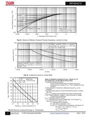
Avalanche Characteristics
E
AS (Thermally limited)
Single Pulse Avalanche Energy
149
mJ
E
AS (Thermally limited)
Single Pulse Avalanche Energy
370
I
AR
Avalanche Current
See Fig 15, 16, 23a, 23b
A
E
AR
Repetitive Avalanche Energy mJ
Thermal Resistance
Symbol Parameter Typ. Max. Units
R
JC
(Bottom)
Junction-to-Case
––– 1.0
R
JC
(Top)
Junction-to-Case
––– 18
°C/W
R
JA
Junction-to-Ambient
––– 33
R
JA
(<10s)
Junction-to-Ambient
––– 20
器件 Datasheet 文档搜索
AiEMA 数据库涵盖高达 72,405,303 个元件的数据手册,每天更新 5,000 多个 PDF 文件
