Datasheet 搜索 > MOS管 > International Rectifier(国际整流器) > IRFR3710ZTRLPBF 数据手册 > IRFR3710ZTRLPBF 数据手册 2/12 页

¥ 7.239
IRFR3710ZTRLPBF 数据手册 - International Rectifier(国际整流器)
制造商:
International Rectifier(国际整流器)
分类:
MOS管
封装:
TO-252-3
Pictures:
3D模型
符号图
焊盘图
引脚图
产品图
页面导航:
封装尺寸在P9P10P11
标记信息在P9P10
技术参数、封装参数在P1
电气规格在P2
导航目录
IRFR3710ZTRLPBF数据手册
Page:
of 12 Go
若手册格式错乱,请下载阅览PDF原文件
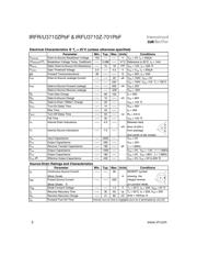
IRFR/U3710ZPbF & IRFU3710Z-701PbF
2 www.irf.com
S
D
G
S
D
G
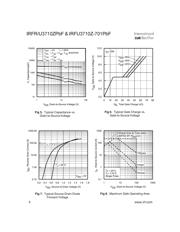
Electrical Characteristics @ T
J
= 25°C (unless otherwise specified)
Parameter Min. Typ. Max. Units
V
(BR)DSS
Drain-to-Source Breakdown Voltage 100 ––– ––– V
∆
V
(BR)DSS
/
∆
T
J
Breakdown Voltage Temp. Coefficient ––– 0.088 ––– V/°C
R
DS(on)
Static Drain-to-Source On-Resistance ––– 15 18
m
Ω
V
GS(th)
Gate Threshold Voltage 2.0 ––– 4.0 V
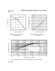
gfs Forward Transconductance 39 ––– ––– S
I
DSS
Drain-to-Source Leakage Current ––– ––– 20 µA
––– ––– 250
I
GSS
Gate-to-Source Forward Leakage ––– ––– 200 nA
Gate-to-Source Reverse Leakage ––– ––– -200
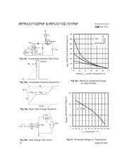
Q
g
Total Gate Charge ––– 69 100
Q
gs
Gate-to-Source Charge ––– 15 ––– nC
Q
gd
Gate-to-Drain ("Miller") Charge ––– 25 –––
t
d(on)
Turn-On Delay Time ––– 14 –––
t
r
Rise Time ––– 43 –––
t
d(off)
Turn-Off Delay Time ––– 53 ––– ns
t
f
Fall Time ––– 42 –––
L
D
Internal Drain Inductance ––– 4.5 ––– Between lead,
nH 6mm (0.25in.)
L
S
Internal Source Inductance ––– 7.5 ––– from package
and center of die contact
C
iss
Input Capacitance ––– 2930 –––
C
oss
Output Capacitance ––– 290 –––
C
rss
Reverse Transfer Capacitance ––– 180 ––– pF
C
oss
Output Capacitance ––– 1200 –––
C
oss
Output Capacitance ––– 180 –––
C
oss
eff.
Effective Output Capacitance ––– 430 –––
Source-Drain Ratin
g
s and Characteristics
Parameter Min. Typ. Max. Units
I
S
Continuous Source Current ––– ––– 56
(Body Diode) A
I
SM
Pulsed Source Current ––– ––– 220
(Body Diode)
c
V
SD
Diode Forward Voltage ––– ––– 1.3 V
t
rr
Reverse Recovery Time ––– 35 53 ns
Q
rr
Reverse Recovery Charge ––– 41 62 nC
t
on
Forward Turn-On Time Intrinsic turn-on time is negligible (turn-on is dominated by LS+LD)
V
GS
= 0V, V
DS
= 1.0V, ƒ = 1.0MHz
V
GS
= 0V, V
DS
= 80V, ƒ = 1.0MHz
V
GS
= 0V, V
DS
= 0V to 80V
f
V
GS
= 10V
e
V
DD
= 50V
I
D
= 33A
R
G
= 6.8
Ω
T
J
= 25°C, I
S
= 33A, V
GS
= 0V
e
T
J
= 25°C, I
F
= 33A, V
DD
= 50V
di/dt = 100A/µs
e
Conditions
V
GS
= 0V, I
D
= 250µA
Reference to 25°C, I
D
= 1mA
V
GS
= 10V, I
D
= 33A
e
V
DS
= V
GS
, I
D
= 250µA
V
DS
= 100V, V
GS
= 0V
V
DS
= 100V, V
GS
= 0V, T
J
= 125°C
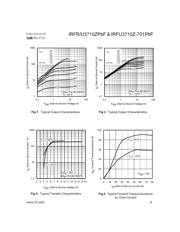
MOSFET symbol
showing the
integral reverse
p-n junction diode.
V
DS
= 25V, I
D
= 33A
I
D
= 33A
V
DS
= 80V
Conditions
V
GS
= 10V
e
V
GS
= 0V
V
DS
= 25V
ƒ = 1.0MHz
V
GS
= 20V
V
GS
= -20V
器件 Datasheet 文档搜索
AiEMA 数据库涵盖高达 72,405,303 个元件的数据手册,每天更新 5,000 多个 PDF 文件
