Datasheet 搜索 > 时钟缓冲器、驱动器、锁相环 > ON Semiconductor(安森美) > NBSG11MNR2G 数据手册 > NBSG11MNR2G 数据手册 2/11 页
 器件3D模型
¥ 40.328
NBSG11MNR2G 数据手册 - ON Semiconductor(安森美)
制造商:
ON Semiconductor(安森美)
分类:
时钟缓冲器、驱动器、锁相环
封装:
QFN-16
描述:
2.5V / 3.3V SiGe半导体1 : 2差分时钟驱动器,带有RSECL输出 2.5V/3.3V SiGe 1:2 Differential Clock Driver with RSECL Outputs
Pictures:
3D模型
符号图
焊盘图
引脚图
产品图
页面导航:


导航目录
NBSG11MNR2G数据手册
Page:
of 11 Go
若手册格式错乱,请下载阅览PDF原文件
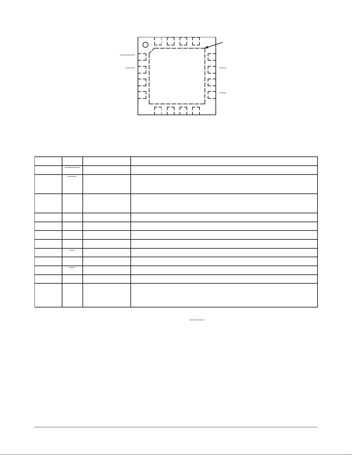
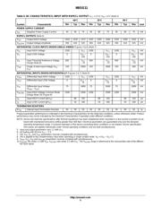
NBSG11
http://onsemi.com
2
V
EE
NC NC V
CC
V
EE
NC NC V
CC
Q0
Q0
Q1
Q1
VTCLK
CLK
CLK
VTCLK
5678
16 15 14 13
12
11
10
9
1
2
3
4
NBSG11
Exposed Pad (EP)
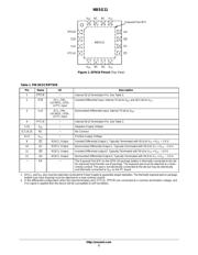
Figure 1. QFN16 Pinout (Top View)
Table 1. PIN DESCRIPTION
Pin Name I/O Description
1 VTCLK −
Internal 50 W Termination Pin. See Table 2.
2 CLK ECL, CML,
LVCMOS, LVDS,
LVTTL Input
Inverted Differential Input. Internal 75 kW to V
EE
and 36.5 kW to V
CC
.
3 CLK ECL, CML,
LVCMOS, LVDS,
LVTTL Input
Noninverted Differential Input. Internal 75 kW to V
EE
.
4 VTCLK −
Internal 50 W Termination Pin. See Table 2.
5,16 V
EE
− Negative Supply Voltage
6,7,14,15 NC − No Connect
8,13 V
CC
− Positive Supply Voltage
9 Q1 RSECL Output
Inverted Differential Output 1. Typically Terminated with 50 W to V
TT
= V
CC
− 2.0 V.
10 Q1 RSECL Output
Noninverted Differential Output 1. Typically Terminated with 50 W to V
TT
= V
CC
− 2.0 V.
11 Q0 RSECL Output
Inverted Differential output 0. Typically Terminated with 50 W to V
TT
= V
CC
− 2.0 V.
12 Q0 RSECL Output
Noninverted Differential Output 0. Typically Terminated with 50 W to V
TT
= V
CC
− 2.0 V.
− EP − The Exposed Pad (EP) on the QFN−16 package bottom is thermally connected to the die
for improved heat transfer out of package. The exposed pad must be attached to a heat−
sinking conduit. The pad is not electrically connected to the die but may be electrically
and thermally connected to V
EE
on the PC board.
1. All V
CC
and V
EE
pins must be externally connected to Power Supply to guarantee proper operation. The thermally exposed pad on package
bottom (see case drawing) must be attached to a heat−sinking conduit.
2. In the differential configuration when the input termination pins (VTCLK, VTCLK
) are connected to a common termination voltage, and
if no signal is applied then the device will be susceptible to self−oscillation.
器件 Datasheet 文档搜索
AiEMA 数据库涵盖高达 72,405,303 个元件的数据手册,每天更新 5,000 多个 PDF 文件
