Datasheet 搜索 > 时钟缓冲器、驱动器、锁相环 > ON Semiconductor(安森美) > NBSG11MNR2G 数据手册 > NBSG11MNR2G 数据手册 5/11 页
 器件3D模型
¥ 40.328
NBSG11MNR2G 数据手册 - ON Semiconductor(安森美)
制造商:
ON Semiconductor(安森美)
分类:
时钟缓冲器、驱动器、锁相环
封装:
QFN-16
描述:
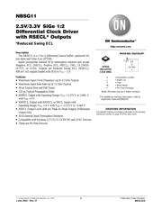
2.5V / 3.3V SiGe半导体1 : 2差分时钟驱动器,带有RSECL输出 2.5V/3.3V SiGe 1:2 Differential Clock Driver with RSECL Outputs
Pictures:
3D模型
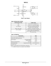
符号图
焊盘图
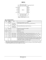
引脚图
产品图
页面导航:

导航目录
NBSG11MNR2G数据手册
Page:
of 11 Go
若手册格式错乱,请下载阅览PDF原文件
NBSG11
http://onsemi.com
5
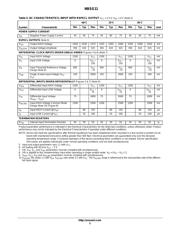
Table 5. DC CHARACTERISTICS, INPUT WITH RSPECL OUTPUT V
CC
= 2.5 V; V
EE
= 0 V (Note 5)
Symbo
l
Characteristic
−40°C 25°C 85°C
Unit
Min Typ Max Min Typ Max Min Typ Max
POWER SUPPLY CURRENT
I
EE
Negative Power Supply Current 45 60 75 45 60 75 45 60 75 mA
RSPECL OUTPUTS (Note 6)
V
OH
Output HIGH Voltage 1450 1530 1575 1525 1565 1600 1550 1590 1625 mV
V
OUTPP
Output Voltage Amplitude 350 410 525 350 410 525 350 410 525 mV
DIFFERENTIAL CLOCK INPUTS DRIVEN SINGLE−ENDED (Figures 4 & 6) (Note 7)
V
IH
Input HIGH Voltage 1200 V
CC
1200 V
CC
1200 V
CC
mV
V
IL
Input LOW Voltage 0 V
IH
−
150
0 V
IH
−
150
0 V
IH
−
150
mV
V
th
Input Threshold Reference Voltage
Range (Note 8)
950 V
CC
–75
950 V
CC
–75
950 V
CC
–75
mV
V
ISE
Single−Ended Input Voltage (V
IH
–
V
IL
)
150 2600 150 2600 150 260 mV
DIFFERENTIAL INPUTS DRIVEN DIFFERENTIALLY (Figures 5 & 7) (Note 9)
V
IHD
Differential Input HIGH Voltage 1200 V
CC
1200 V
CC
1200 V
CC
mV
V
ILD
Differential Input LOW Voltage 0 V
CC
−
75
0 V
CC
−
75
0 V
CC
−
75
mV
V
ID
Differential Input Voltage
(V
IHD
– V
ILD
)
75 2600 75 2600 75 2600 mV
V
IHCMR
Input HIGH Voltage Common Mode
Range (Note 10) (Figure 8)
1200 2500 1200 2500 1200 2500 mV
I
IH
Input HIGH Current (@V
IH
) 80 150 80 150 80 150
mA
I
IL
Input LOW Current (@V
IL
) 25 100 25 100 25 100
mA
TERMINATION RESISTORS
R
TIN
Internal Input Termination Resistor 45 50 55 45 50 55 45 50 55
W
Product parametric performance is indicated in the Electrical Characteristics for the listed test conditions, unless otherwise noted. Product
performance may not be indicated by the Electrical Characteristics if operated under different conditions.
NOTE: Device will meet the specifications after thermal equilibrium has been established when mounted in a test socket or printed circuit
board with maintained transverse airflow greater than 500 lfpm. Electrical parameters are guaranteed only over the declared
operating temperature range. Functional operation of the device exceeding these conditions is not implied. Device specification
limit values are applied individually under normal operating conditions and not valid simultaneously.
5. Input and output parameters vary 1:1 with V
CC
.
6. All loading with 50 W to V
CC
− 2 V.
7. Vth, V
IH
, V
IL,
and V
ISE
parameters must be complied with simultaneously.
8. Vth is applied to the complementary input when operating in single−ended mode. V
th
= (V
IH
− V
IL
) / 2.
9. V
IHD
, V
ILD,
V
ID
and V
IHCMR
parameters must be complied with simultaneously.
10.V
IHCMR
min varies 1:1 with V
EE
, V
IHCMR
max varies 1:1 with V
CC
. The V
IHCMR
range is referenced to the most positive side of the differen-
tial input signal.
器件 Datasheet 文档搜索
AiEMA 数据库涵盖高达 72,405,303 个元件的数据手册,每天更新 5,000 多个 PDF 文件
