Datasheet 搜索 > 时钟缓冲器、驱动器、锁相环 > ON Semiconductor(安森美) > NBSG11MNR2G 数据手册 > NBSG11MNR2G 数据手册 4/11 页
 器件3D模型
¥ 40.328
NBSG11MNR2G 数据手册 - ON Semiconductor(安森美)
制造商:
ON Semiconductor(安森美)
分类:
时钟缓冲器、驱动器、锁相环
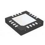
封装:
QFN-16
描述:
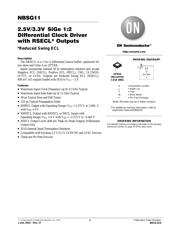
2.5V / 3.3V SiGe半导体1 : 2差分时钟驱动器,带有RSECL输出 2.5V/3.3V SiGe 1:2 Differential Clock Driver with RSECL Outputs
Pictures:
3D模型
符号图
焊盘图
引脚图
产品图
页面导航:

导航目录
NBSG11MNR2G数据手册
Page:
of 11 Go
若手册格式错乱,请下载阅览PDF原文件
NBSG11
http://onsemi.com
4
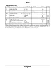
Table 4. MAXIMUM RATINGS
Symbol Parameter Condition 1 Condition 2 Rating Unit
V
CC
Positive Power Supply V
EE
= 0 V 3.6 V
V
EE
Negative Power Supply V
CC
= 0 V −3.6 V
V
I
Positive Input
Negative Input
V
EE
= 0 V
V
CC
= 0 V
V
I
≤ V
CC
V
I
≥ V
EE
3.6
−3.6
V
V
V
INPP
Differential Input Voltage |D − D| V
CC
− V
EE
w 2.8 V
V
CC
− V
EE
< 2.8 V
2.8
|V
CC
− V
EE
|
V
V
I
out
Output Current Continuous
Surge
25
50
mA
mA
T
A
Operating Temperature Range −40 to +85 °C
T
stg
Storage Temperature Range −65 to +150 °C
q
JA
Thermal Resistance (Junction−to−Ambient)
(Note 4)
0 lfpm
500 lfpm
41.6
35.2
°C/W
°C/W
q
JC
Thermal Resistance (Junction−to−Case) 2S2P (Note 4) 4.0 °C/W
T
sol
Wave Solder Pb−Free 265 °C
Stresses exceeding Maximum Ratings may damage the device. Maximum Ratings are stress ratings only. Functional operation above the
Recommended Operating Conditions is not implied. Extended exposure to stresses above the Recommended Operating Conditions may affect
device reliability.
4. JEDEC standard multilayer board − 2S2P (2 signal, 2 power) with 8 filled thermal vias under exposed pad.
器件 Datasheet 文档搜索
AiEMA 数据库涵盖高达 72,405,303 个元件的数据手册,每天更新 5,000 多个 PDF 文件
