Datasheet 搜索 > MOS管 > ON Semiconductor(安森美) > NTD3055L104 数据手册 > NTD3055L104 数据手册 2/8 页

¥ 1.599
NTD3055L104 数据手册 - ON Semiconductor(安森美)
制造商:
ON Semiconductor(安森美)
分类:
MOS管
封装:
TO-252-3
描述:
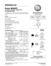
60V,12A,逻辑电平N沟道功率MOSFET
Pictures:
3D模型
符号图
焊盘图
引脚图
产品图
页面导航:
导航目录
NTD3055L104数据手册
Page:
of 8 Go
若手册格式错乱,请下载阅览PDF原文件
NTD3055L104
http://onsemi.com
2
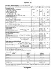
ELECTRICAL CHARACTERISTICS (T
J
= 25°C unless otherwise noted)
Characteristic Symbol Min Typ Max Unit
OFF CHARACTERISTICS
Drain−to−Source Breakdown Voltage (Note 3)
(V
GS
= 0 Vdc, I
D
= 250 mAdc)
Temperature Coefficient (Positive)
V
(BR)DSS
60
−
70
62.9
−
−
Vdc
mV/°C
Zero Gate Voltage Drain Current
(V
DS
= 60 Vdc, V
GS
= 0 Vdc)
(V
DS
= 60 Vdc, V
GS
= 0 Vdc, T
J
= 150°C)
I
DSS
−
−
−
−
1.0
10
mAdc
Gate−Body Leakage Current (V
GS
= ± 15 Vdc, V
DS
= 0 Vdc) I
GSS
− − ±100 nAdc
ON CHARACTERISTICS (Note 3)
Gate Threshold Voltage (Note 3)
(V
DS
= V
GS
, I
D
= 250 mAdc)
Threshold Temperature Coefficient (Negative)
V
GS(th)
1.0
−
1.6
4.2
2.0
−
Vdc
mV/°C
Static Drain−to−Source On−Resistance (Note 3)
(V
GS
= 5.0 Vdc, I
D
= 6.0 Adc)
R
DS(on)
− 89 104
mW
Static Drain−to−Source On−Voltage (Note 3)
(V
GS
= 5.0 Vdc, I
D
= 12 Adc)
(V
GS
= 5.0 Vdc, I
D
= 6.0 Adc, T
J
= 150°C)
V
DS(on)
−
−
0.98
0.86
1.50
−
Vdc
Forward Transconductance (Note 3) (V
DS
= 8.0 Vdc, I
D
= 6.0 Adc) g
FS
− 9.1 − mhos
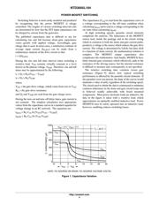
DYNAMIC CHARACTERISTICS
Input Capacitance
(V 25 Vdc V 0 Vdc
C
iss
− 316 440 pF
Output Capacitance
(V
DS
= 25 Vdc, V
GS
= 0 Vdc,
f = 1.0 MHz
)
C
oss
− 105 150
Transfer Capacitance
f = 1
.
0 MHz)
C
rss
− 35 70
SWITCHING CHARACTERISTICS (Note 4)
Turn−On Delay Time t
d(on)
− 9.2 20 ns
Rise Time
(V
DD
= 30 Vdc, I
D
= 12 Adc,
t
r
− 104 210
Turn−Off Delay Time
(V
DD
30 Vdc, I
D
12 Adc,
V
GS
= 5.0 Vdc, R
G
= 9.1 W) (Note 3)
t
d(off)
− 19 40
Fall Time
GS G
t
f
− 40.5 80
Gate Charge
(V 48 Vdc I 12 Adc
Q
T
− 7.4 20 nC
g
(V
DS
= 48 Vdc, I
D
= 12 Adc,
V
GS
= 5 0 Vdc) (Note 3)
Q
1
− 2.0 −
V
GS
=
5
.
0 Vd
c
) (N
o
t
e
3)
Q
2
− 4.0 −
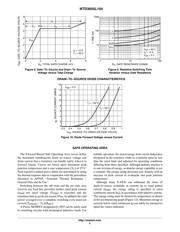
SOURCE−DRAIN DIODE CHARACTERISTICS
Forward On−Voltage (I
S
= 12 Adc, V
GS
= 0 Vdc) (Note 3)
(I
S
= 12 Adc, V
GS
= 0 Vdc, T
J
= 150°C)
V
SD
−
−
0.95
0.82
1.2
−
Vdc
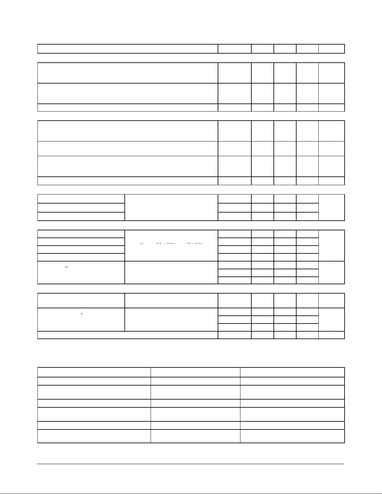
Reverse Recovery Time
(I 12 Adc V 0 Vdc
t
rr
− 35 −
ns
y
(I
S
= 12 Adc, V
GS
= 0 Vdc,
dI
S
/dt = 100 A/ms) (Note 3)
t
a
− 21 −
dI
S
/dt
=
100 A/
ms
) (N
o
t
e
3)
t
b
− 14 −
Reverse Recovery Stored Charge Q
RR
− 0.04 −
mC
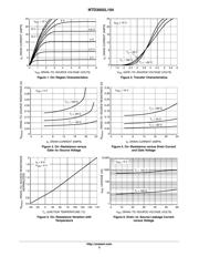
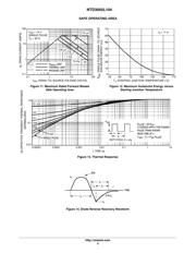
3. Pulse Test: Pulse Width ≤ 300 ms, Duty Cycle ≤ 2%.
4. Switching characteristics are independent of operating junction temperatures.
ORDERING INFORMATION
Device Package Shipping
†
NTD3055L104 DPAK 75 Units/Rail
NTD3055L104G DPAK
(Pb−Free)
75 Units/Rail
NTD3055L104−1 DPAK−3 75 Units/Rail
NTD3055L104−1G DPAK−3
(Pb−Free)
75 Units/Rail
NTD3055L104T4 DPAK 2500 Tape & Reel
NTD3055L104T4G DPAK
(Pb−Free)
2500 Tape & Reel
†For information on tape and reel specifications, including part orientation and tape sizes, please refer to our Tape and Reel Packaging
Specifications Brochure, BRD8011/D.
器件 Datasheet 文档搜索
AiEMA 数据库涵盖高达 72,405,303 个元件的数据手册,每天更新 5,000 多个 PDF 文件
