Datasheet 搜索 > MOS管 > ON Semiconductor(安森美) > NTD3055L104 数据手册 > NTD3055L104 数据手册 4/8 页

¥ 1.599
NTD3055L104 数据手册 - ON Semiconductor(安森美)
制造商:
ON Semiconductor(安森美)
分类:
MOS管
封装:
TO-252-3
描述:
60V,12A,逻辑电平N沟道功率MOSFET
Pictures:
3D模型
符号图
焊盘图
引脚图
产品图
页面导航:

导航目录
NTD3055L104数据手册
Page:
of 8 Go
若手册格式错乱,请下载阅览PDF原文件
NTD3055L104
http://onsemi.com
4
POWER MOSFET SWITCHING
Switching behavior is most easily modeled and predicted
by recognizing that the power MOSFET is charge
controlled. The lengths of various switching intervals (Dt)
are determined by how fast the FET input capacitance can
be charged by current from the generator.
The published capacitance data is difficult to use for
calculating rise and fall because drain−gate capacitance
varies greatly with applied voltage. Accordingly, gate
charge data is used. In most cases, a satisfactory estimate of
average input current (I
G(AV)
) can be made from a
rudimentary analysis of the drive circuit so that
t = Q/I
G(AV)
During the rise and fall time interval when switching a
resistive load, V
GS
remains virtually constant at a level
known as the plateau voltage, V
SGP
. Therefore, rise and fall
times may be approximated by the following:
t
r
= Q
2
x R
G
/(V
GG
− V
GSP
)
t
f
= Q
2
x R
G
/V
GSP
where
V
GG
= the gate drive voltage, which varies from zero to V
GG
R
G
= the gate drive resistance
and Q
2
and V
GSP
are read from the gate charge curve.
During the turn−on and turn−off delay times, gate current is
not constant. The simplest calculation uses appropriate
values from the capacitance curves in a standard equation for
voltage change in an RC network. The equations are:
t
d(on)
= R
G
C
iss
In [V
GG
/(V
GG
− V
GSP
)]
t
d(off)
= R
G
C
iss
In (V
GG
/V
GSP
)
The capacitance (C
iss
) is read from the capacitance curve at
a voltage corresponding to the off−state condition when
calculating t
d(on)
and is read at a voltage corresponding to the
on−state when calculating t
d(off)
.
At high switching speeds, parasitic circuit elements
complicate the analysis. The inductance of the MOSFET
source lead, inside the package and in the circuit wiring
which is common to both the drain and gate current paths,
produces a voltage at the source which reduces the gate drive
current. The voltage is determined by Ldi/dt, but since di/dt
is a function of drain current, the mathematical solution is
complex. The MOSFET output capacitance also
complicates the mathematics. And finally, MOSFETs have
finite internal gate resistance which effectively adds to the
resistance of the driving source, but the internal resistance
is difficult to measure and, consequently, is not specified.
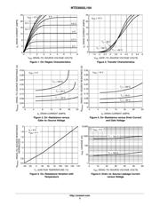
The resistive switching time variation versus gate
resistance (Figure 9) shows how typical switching
performance is affected by the parasitic circuit elements. If
the parasitics were not present, the slope of the curves would
maintain a value of unity regardless of the switching speed.
The circuit used to obtain the data is constructed to minimize
common inductance in the drain and gate circuit loops and
is believed readily achievable with board mounted
components. Most power electronic loads are inductive; the
data in the figure is taken with a resistive load, which
approximates an optimally snubbed inductive load. Power
MOSFETs may be safely operated into an inductive load;
however, snubbing reduces switching losses.
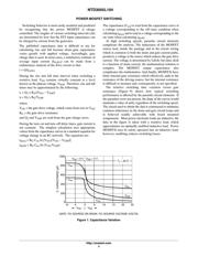
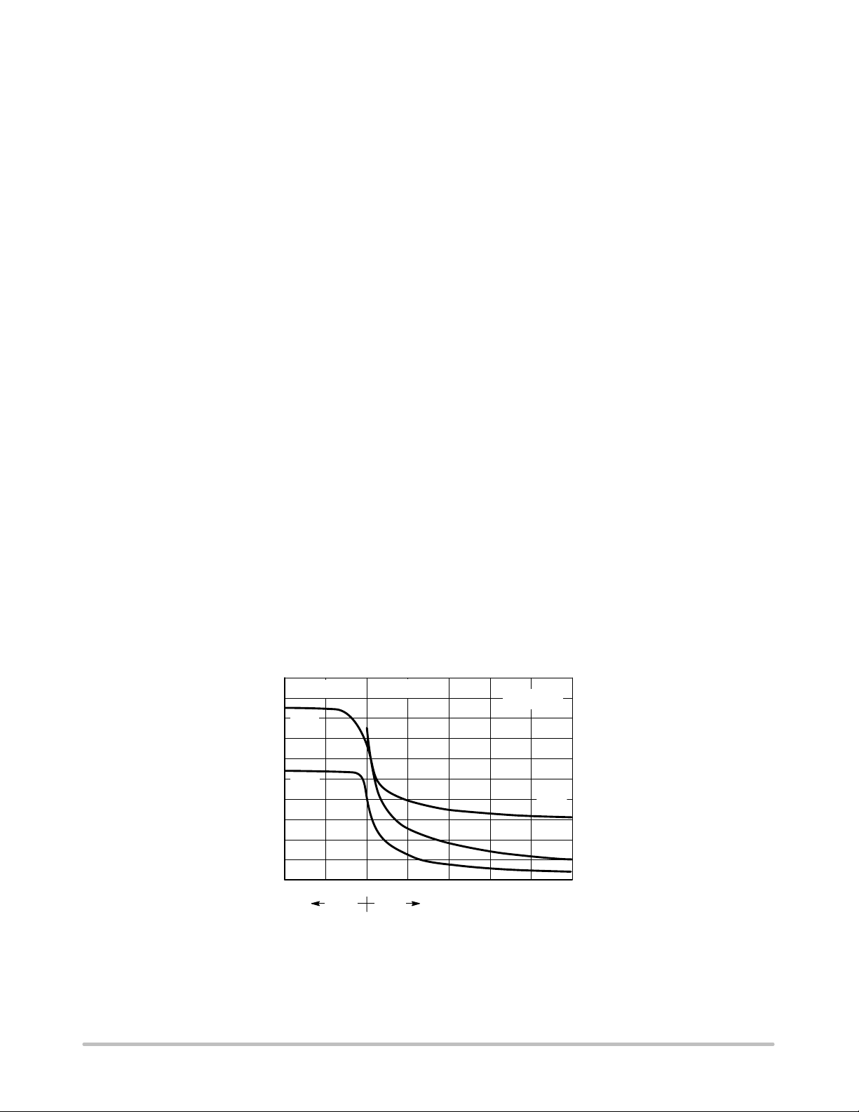
C
rss
10 0 10 15 20 25
GATE−TO−SOURCE OR DRAIN−TO−SOURCE VOLTAGE (VOLTS)
C, CAPACITANCE (pF)
Figure 7. Capacitance Variation
1000
200
0
V
GS
V
DS
400
55
V
GS
= 0 VV
DS
= 0 V
T
J
= 25°C
C
iss
C
oss
C
rss
C
iss
600
800
器件 Datasheet 文档搜索
AiEMA 数据库涵盖高达 72,405,303 个元件的数据手册,每天更新 5,000 多个 PDF 文件
