Datasheet 搜索 > MOS管 > ON Semiconductor(安森美) > NTD3055L104 数据手册 > NTD3055L104 数据手册 5/8 页


¥ 1.599
NTD3055L104 数据手册 - ON Semiconductor(安森美)
制造商:
ON Semiconductor(安森美)
分类:
MOS管
封装:
TO-252-3
描述:
60V,12A,逻辑电平N沟道功率MOSFET
Pictures:
3D模型
符号图
焊盘图
引脚图
产品图
页面导航:

导航目录
NTD3055L104数据手册
Page:
of 8 Go
若手册格式错乱,请下载阅览PDF原文件
NTD3055L104
http://onsemi.com
5
16
0
0.3
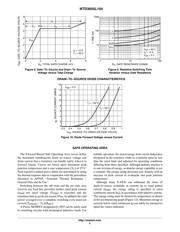
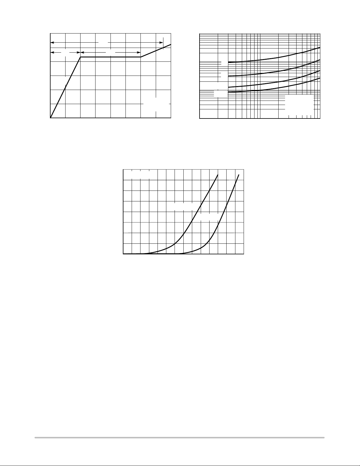
DRAIN−TO−SOURCE DIODE CHARACTERISTICS
V
SD
, SOURCE−TO−DRAIN VOLTAGE (VOLTS)
Figure 8. Gate−To−Source and Drain−To−Source
Voltage versus Total Charge
I
S
, SOURCE CURRENT (AMPS)
Figure 9. Resistive Switching Time
Variation versus Gate Resistance
R
G
, GATE RESISTANCE (OHMS)
1 10 100
1000
1
t, TIME (ns)
V
GS
= 0 V
Figure 10. Diode Forward Voltage versus Current
V
GS
, GATE−TO−SOURCE VOLTAGE (VOLTS)
0
5
3
1
0
Q
G
, TOTAL GATE CHARGE (nC)
6
4
2
4
100
28
0.5 1
2
4
6
I
D
= 12 A
T
J
= 25°C
V
GS
Q
2
Q
1
Q
T
t
r
t
d(off)
t
d(on)
t
f
10
V
DS
= 30 V
I
D
= 12 A
V
GS
= 5 V
0.7 0.9
6
8
0.80.60.4
10
12
14
T
J
= 150°C
T
J
= 25°C
SAFE OPERATING AREA
The Forward Biased Safe Operating Area curves define
the maximum simultaneous drain−to−source voltage and
drain current that a transistor can handle safely when it is
forward biased. Curves are based upon maximum peak
junction temperature and a case temperature (T
C
) of 25°C.
Peak repetitive pulsed power limits are determined by using
the thermal response data in conjunction with the procedures
discussed in AN569, “Transient Thermal Resistance −
General Data and Its Use.”
Switching between the off−state and the on−state may
traverse any load line provided neither rated peak current
(I
DM
) nor rated voltage (V
DSS
) is exceeded and the
transition time (t
r
,t
f
) do not exceed 10 ms. In addition the total
power averaged over a complete switching cycle must not
exceed (T
J(MAX)
− T
C
)/(R
qJC
).
A Power MOSFET designated E−FET can be safely used
in switching circuits with unclamped inductive loads. For
reliable operation, the stored energy from circuit inductance
dissipated in the transistor while in avalanche must be less
than the rated limit and adjusted for operating conditions
differing from those specified. Although industry practice is
to rate in terms of energy, avalanche energy capability is not
a constant. The energy rating decreases non−linearly with an
increase of peak current in avalanche and peak junction
temperature.
Although many E−FETs can withstand the stress of
drain−to−source avalanche at currents up to rated pulsed
current (I
DM
), the energy rating is specified at rated
continuous current (I
D
), in accordance with industry custom.
The energy rating must be derated for temperature as shown
in the accompanying graph (Figure 12). Maximum energy at
currents below rated continuous I
D
can safely be assumed to
equal the values indicated.
器件 Datasheet 文档搜索
AiEMA 数据库涵盖高达 72,405,303 个元件的数据手册,每天更新 5,000 多个 PDF 文件
