Datasheet 搜索 > 微控制器 > Renesas Electronics(瑞萨电子) > R5F52105BDFM#30 数据手册 > R5F52105BDFM#30 数据手册 5/223 页
 器件3D模型
¥ 38.656
R5F52105BDFM#30 数据手册 - Renesas Electronics(瑞萨电子)
制造商:
Renesas Electronics(瑞萨电子)
分类:
微控制器
封装:
LFQFP-64
描述:
RX210 微控制器RX210 低功率微控制器具有宽工作范围并且可以在高达 50 MHz 78 DMIPS 时执行计算。 使用 RX210 的应用包括数码相机、洗衣机、功率计、智能手机、医疗保健设备和冰箱。工作范围:1.62 V 至 5.3 V 事件链接控制器 (ELC) 多功能引脚控制器 (MPC) 三相电动机控制计时器 (MTU2) 12 位模/数转换器 4 种功耗模式: -睡眠模式 -所有模块时钟停止模式 -软件待机模式 -深度软件待机模式 ### RX 系列微控制器,Renesas ElectronicsRX 系列 32 位闪存微控制器持续发展,用于工业、消费品和办公自动化应用。
Pictures:
3D模型
符号图
焊盘图
引脚图
产品图
页面导航:
引脚图在P14P15P16P17P18P19P20P21P22P23P24P25Hot
原理图在P13
封装尺寸在P18P20P23P24P207P208P209P210P211P212P213P214
功能描述在P2P3P4P5P6
技术参数、封装参数在P2P3P4P5P6P87
应用领域在P1
电气规格在P87P88P89P90P91P92P93P94P95P96P97P98
导航目录
R5F52105BDFM#30数据手册
Page:
of 223 Go
若手册格式错乱,请下载阅览PDF原文件

R01DS0041EJ0150 Rev.1.50 Page 5 of 221
Oct 18, 2013
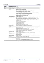
RX210 Group 1. Overview
Communication
functions
Serial communications
interfaces (SCIc, SCId)
13 channels (channel 0 to 11: SCIc, channel 12: SCId)
Serial communications modes:
Asynchronous, clock synchronous, and smart-card interface
On-chip baud rate generator allows selection of the desired bit rate
Choice of LSB-first or MSB-first transfer
Average transfer rate clock can be input from TMR timers (SCI5, SCI6, and SCI12)
Simple IIC
Simple SPI
Master/slave mode supported (SCId only)
Start frame and information frame are included (SCId only)
I
2
C bus interface (RIIC)
1 channel
Communications formats:
I
2
C bus format/SMBus format
Master/slave selectable
Supports the fast mode
Serial peripheral
interface (RSPI)
1 channel
Transfer facility
Using the MOSI (master out, slave in), MISO (master in, slave out), SSL (slave select), and RSPI
clock (RSPCK) signals enables serial transfer through SPI operation (four lines) or clock-
synchronous operation (three lines)
Capable of handling serial transfer as a master or slave
Data formats
Choice of LSB-first or MSB-first transfer
The number of bits in each transfer can be changed to any number of bits from 8 to 16, 20, 24, or 32
bits.
128-bit buffers for transmission and reception
Up to four frames can be transmitted or received in a single transfer operation (with each frame
having up to 32 bits)
Double buffers for both transmission and reception
12-bit A/D converter (S12ADb)
12 bits (16 channels 1 unit)
12-bit resolution
Minimum conversion time: 1.0 s per channel (in operation with ADCLK at 50 MHz)
Operating modes
Scan mode (single scan mode, continuous scan mode, and group scan mode)
Sample-and-hold function
Self-diagnosis for the A/D converter
Assistance in detecting disconnected analog inputs
Double-trigger mode (duplication of A/D conversion data)
A/D conversion start conditions
A software trigger, a trigger from a timer (MTU), an external trigger signal, or ELC
Temperature sensor (TEMPSa)
Outputs the voltage that changes depending on the temperature
PGA gain switchable: Four levels according to the voltage range
D/A converter (DA)
2 channels
10-bit resolution
Output voltage: 0 V to VREFH
CRC calculator (CRC)
CRC code generation for arbitrary amounts of data in 8-bit units
Select any of three generating polynomials:
X
8
+ X
2
+ X + 1, X
16
+ X
15
+ X
2
+ 1, or X
16
+ X
12
+ X
5
+ 1
Generation of CRC codes for use with LSB-first or MSB-first communications is selectable.
Comparator A (CMPA)
2 channels
Comparison of reference voltage and analog input voltage
Comparator B (CMPB)
2 channels
Comparison of reference voltage and analog input voltage
Data Operation Circuit (DOC) Comparison, addition, and subtraction of 16-bit data
Power supply voltage/Operating frequency VCC = 1.62 to 1.8 V: 20 MHz, VCC = 1.8 to 2.7 V: 32 MHz, VCC = 2.7 to 5.5 V: 50 MHz
Operating temperature D version: 40 to +85C, G version: 40 to +105C*
2
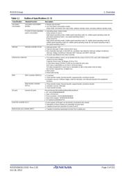
Table 1.1 Outline of Specifications (4 / 5)
Classification Module/Function Description
器件 Datasheet 文档搜索
AiEMA 数据库涵盖高达 72,405,303 个元件的数据手册,每天更新 5,000 多个 PDF 文件
