Datasheet 搜索 > Flash芯片 > Spansion(飞索半导体) > S29GL032N90TFI040 数据手册 > S29GL032N90TFI040 数据手册 3/83 页
 器件3D模型
¥ 5.212
S29GL032N90TFI040 数据手册 - Spansion(飞索半导体)
制造商:
Spansion(飞索半导体)
分类:
Flash芯片
封装:
TSOP-48
描述:
SPANSION S29GL032N90TFI040 闪存, 32 Mbit, 4M x 8位 / 2M x 16位, CFI, TSOP, 48 引脚
Pictures:
3D模型
符号图
焊盘图
引脚图
产品图
页面导航:
引脚图在P10Hot
原理图在P5
封装尺寸在P75P81
型号编码规则在P1P3P13P15P37P81
封装信息在P13P15
功能描述在P3
技术参数、封装参数在P1P60P63
电气规格在P2
型号编号列表在P1

导航目录
S29GL032N90TFI040数据手册
Page:
of 83 Go
若手册格式错乱,请下载阅览PDF原文件

Document Number: 001-98525 Rev. *A Page 3 of 83
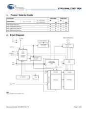
S29GL064N, S29GL032N
General Description
The S29GL-N family of devices are 3.0-Volt single-power Flash memory manufactured using 110 nm MirrorBit technology. The
S29GL064N is a 64-Mb device organized as 4,194,304 words or 8,388,608 bytes. The S29GL032N is a 32-Mb device organized as
2,097,152 words or 4,194,304 bytes. Depending on the model number, the devices have 16-bit wide data bus only, or a 16-bit wide
data bus that can also function as an 8-bit wide data bus by using the BYTE# input. The devices can be programmed either in the
host system or in standard EPROM programmers.
Access times as fast as 90 ns are available. Note that each access time has a specific operating voltage range (V
CC
) as specified in
the Product Selector Guide and the Ordering Information–S29GL032N, and Ordering Information–S29GL064N. Package offerings
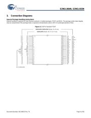
include 48-pin TSOP, 56-pin TSOP, 48-ball fine-pitch BGA and 64-ball Fortified BGA, depending on model number. Each device has
separate chip enable (CE#), write enable (WE#) and output enable (OE#) controls.
Each device requires only a single 3.0-Volt power supply for both read and write functions. In addition to a V
CC
input, a high-
voltage accelerated program (ACC) feature provides shorter programming times through increased voltage on the WP#/ACC or
ACC input. This feature is intended to facilitate factory throughput during system production, but may also be used in the field if
desired.
The device is entirely command set compatible with the JEDEC single-power-supply Flash standard. Commands are written to
the device using standard microprocessor write timing. Write cycles also internally latch addresses and data needed for the
programming and erase operations.
The sector erase architecture allows memory sectors to be erased and reprogrammed without affecting the data contents of other
sectors. The device is fully erased when shipped from the factory.
The Advanced Sector Protection features several levels of sector protection, which can disable both the program and erase
operations in certain sectors. Persistent Sector Protection is a method that replaces the previous 12-volt controlled protection
method. Password Sector Protection is a highly sophisticated protection method that requires a password before changes to certain
sectors are permitted.
Device programming and erasure are initiated through command sequences. Once a program or erase operation begins, the host
system need only poll the DQ7 (Data# Polling) or DQ6 (toggle) status bits or monitor the Ready/Busy# (RY/BY#) output to
determine whether the operation is complete. To facilitate programming, an Unlock Bypass mode reduces command sequence
overhead by requiring only two write cycles to program data instead of four.
Hardware data protection measures include a low V
CC
detector that automatically inhibits write operations during power
transitions. The hardware sector protection feature disables both program and erase operations in any combination of sectors of
memory. This can be achieved in-system or via programming equipment.
The Erase Suspend/Erase Resume feature allows the host system to pause an erase operation in a given sector to read or
program any other sector and then complete the erase operation. The Program Suspend/Program Resume feature enables the
host system to pause a program operation in a given sector to read any other sector and then complete the program operation.
The hardware RESET# pin terminates any operation in progress and resets the device, after which it is then ready for a new
operation. The RESET# pin may be tied to the system reset circuitry. A system reset would thus also reset the device, enabling the
host system to read boot-up firmware from the Flash memory device.
The device reduces power consumption in the standby mode when it detects specific voltage levels on CE# and RESET#, or when
addresses are stable for a specified period of time.
The Write Protect (WP#) feature protects the first or last sector by asserting a logic low on the WP#/ACC pin or WP# pin, depending
on model number. The protected sector is still protected even during accelerated programming.
The Secured Silicon Sector provides a 128-word/256-byte area for code or data that can be permanently protected. Once this
sector is protected, no further changes within the sector can occur.
Cypress MirrorBit flash technology combines years of Flash memory manufacturing experience to produce the highest levels of
quality, reliability and cost effectiveness. The device electrically erases all bits within a sector simultaneously via hot-hole assisted
erase. The data is programmed using hot electron injection.
器件 Datasheet 文档搜索
AiEMA 数据库涵盖高达 72,405,303 个元件的数据手册,每天更新 5,000 多个 PDF 文件
