Datasheet 搜索 > Flash芯片 > Spansion(飞索半导体) > S29GL032N90TFI040 数据手册 > S29GL032N90TFI040 数据手册 4/83 页
 器件3D模型
¥ 5.212
S29GL032N90TFI040 数据手册 - Spansion(飞索半导体)
制造商:
Spansion(飞索半导体)
分类:
Flash芯片
封装:
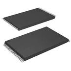
TSOP-48
描述:
SPANSION S29GL032N90TFI040 闪存, 32 Mbit, 4M x 8位 / 2M x 16位, CFI, TSOP, 48 引脚
Pictures:
3D模型
符号图
焊盘图
引脚图
产品图
页面导航:
引脚图在P10Hot
原理图在P5
封装尺寸在P75P81
型号编码规则在P1P3P13P15P37P81
封装信息在P13P15
功能描述在P3
技术参数、封装参数在P1P60P63
电气规格在P2
型号编号列表在P1
导航目录
S29GL032N90TFI040数据手册
Page:
of 83 Go
若手册格式错乱,请下载阅览PDF原文件

Document Number: 001-98525 Rev. *A Page 4 of 83
S29GL064N, S29GL032N
Table of Contents
Distinctive Characteristics .................................................. 2
General Description ............................................................. 3
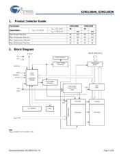
1. Product Selector Guide............................................... 5
2. Block Diagram.............................................................. 5
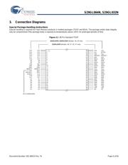
3. Connection Diagrams.................................................. 6
4. Pin Descriptions......................................................... 10
5. Logic Symbols ........................................................... 11
6. Ordering Information–S29GL032N........................... 13
7. Ordering Information–S29GL064N........................... 15
7.1 Valid Combinations...................................................... 15
8. Device Bus Operations.............................................. 16
8.1 Word/Byte Configuration.............................................. 16
8.2 Requirements for Reading Array Data......................... 16
8.3 Writing Commands/Command Sequences.................. 17
8.4 Standby Mode.............................................................. 18
8.5 Automatic Sleep Mode................................................. 18
8.6 RESET#: Hardware Reset Pin..................................... 18
8.7 Output Disable Mode................................................... 18
8.8 Autoselect Mode.......................................................... 28
8.9 Advanced Sector Protection........................................ 30
8.10 Lock Register............................................................... 30
8.11 Persistent Sector Protection ........................................ 31
8.12 Password Sector Protection......................................... 33
8.13 Password and Password Protection Mode Lock Bit .... 33
8.14 Persistent Protection Bit Lock (PPB Lock Bit).............. 34
8.15 Secured Silicon Sector Flash Memory Region ............ 34
8.16 Write Protect (WP#/ACC) ............................................ 35
8.17 Hardware Data Protection............................................ 35
9. Common Flash Memory Interface (CFI)................... 36
10. Command Definitions................................................ 40
10.1 Reading Array Data ..................................................... 40
10.2 Reset Command.......................................................... 40
10.3 Autoselect Command Sequence ................................. 41
10.4 Enter/Exit Secured Silicon Sector
Command Sequence................................................... 41
10.5 Program Suspend/Program Resume
Command Sequence................................................... 45
10.6 Chip Erase Command Sequence ................................ 46
10.7 Sector Erase Command Sequence ............................. 47
10.8 Erase Suspend/Erase Resume Commands................ 49
10.9 Command Definitions................................................... 50
10.10Write Operation Status................................................ 55
10.11DQ7: Data# Polling...................................................... 55
10.12RY/BY#: Ready/Busy# ................................................ 56
10.13DQ6: Toggle Bit I......................................................... 57
10.14DQ2: Toggle Bit II........................................................ 58
10.15Reading Toggle Bits DQ6/DQ2 ................................... 59
10.16DQ5: Exceeded Timing Limits..................................... 59
10.17DQ3: Sector Erase Timer............................................ 59
10.18DQ1: Write-to-Buffer Abort.......................................... 59
11. Absolute Maximum Ratings....................................... 60
12. Operating Ranges....................................................... 61
13. DC Characteristics...................................................... 62
14. Test Conditions........................................................... 63
14.1 Key to Switching Waveforms........................................ 63
15. AC Characteristics...................................................... 64
16. Erase And Programming Performance..................... 73
17. Physical Dimensions.................................................. 75
17.1 TS048—48-Pin Standard Thin Small
Outline Package (TSOP).............................................. 75
17.2 TS056—56-Pin Standard Thin Small
Outline Package (TSOP).............................................. 76
17.3 VBK048—Ball Fine-pitch Ball
Grid Array (BGA) 8.15x 6.15 mm Package................... 77
17.4 LAA064—64-Ball Fortified Ball
Grid Array (BGA) 13 x 11 mm Package........................ 78
17.5 LAE064-64-Ball Fortified Ball
Grid Array (BGA) 9 x 9 mm Package............................ 79
18. Revision History.......................................................... 80
器件 Datasheet 文档搜索
AiEMA 数据库涵盖高达 72,405,303 个元件的数据手册,每天更新 5,000 多个 PDF 文件
