Datasheet 搜索 > MOS管 > VISHAY(威世) > SI4421DY-T1-E3 数据手册 > SI4421DY-T1-E3 数据手册 2/8 页
 器件3D模型
¥ 12.247
SI4421DY-T1-E3 数据手册 - VISHAY(威世)
制造商:
VISHAY(威世)
分类:
MOS管
封装:
SOIC-8
描述:
SI4421DY-T1-E3 编带
Pictures:
3D模型
符号图
焊盘图
引脚图
产品图
SI4421DY-T1-E3数据手册
Page:
of 8 Go
若手册格式错乱,请下载阅览PDF原文件
www.vishay.com
2
Document Number: 72114
S-82282-Rev. C, 22-Sep-08
Vishay Siliconix
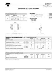
Si4421DY
Notes:
a. Pulse test; pulse width ≤ 300 µs, duty cycle ≤ 2 %.
b. Guaranteed by design, not subject to production testing.
Stresses beyond those listed under “Absolute Maximum Ratings” may cause permanent damage to the device. These are stress ratings only, and functional operation
of the device at these or any other conditions beyond those indicated in the operational sections of the specifications is not implied. Exposure to absolute maximum
rating conditions for extended periods may affect device reliability.
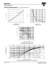
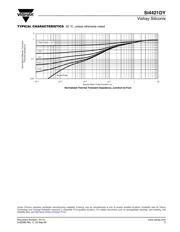
TYPICAL CHARACTERISTICS 25 °C, unless otherwise noted
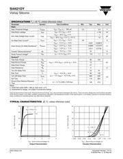
SPECIFICATIONS T
J
= 25 °C, unless otherwise noted
Parameter Symbol Test Conditions Min. Typ. Max. Unit
Static
Gate Threshold Voltage
V
GS(th)
V
DS
= V
GS
, I
D
= - 850 µA
- 0.4 - 0.8 V
Gate-Body Leakage
I
GSS
V
DS
= 0 V, V
GS
= ± 8 V
± 100 nA
Zero Gate Voltage Drain Current
I
DSS
V
DS
= - 20 V, V
GS
= 0 V
- 1
µA
V
DS
= - 20 V, V
GS
= 0 V, T
J
= 70 °C
- 10
On-State Drain Current
a
I
D(on)
V
DS
= - 5 V, V
GS
= - 4.5 V
- 30 A
Drain-Source On-State Resistance
a
R
DS(on)
V
GS
= - 4.5 V, I
D
= - 14 A
0.007 0.00875
Ω
V
GS
= - 2.5 V, I
D
= - 12 A
0.0085 0.01075
V
GS
= - 1.8 V, I
D
= - 11 A
0.011 0.0135
Forward Transconductance
a
g
fs
V
DS
= - 10 V, I
D
= - 14 A
55 S
Diode Forward Voltage
a
V
SD
I
S
= - 2.7 A, V
GS
= 0 V
- 0.6 - 1.1 V
Dynamic
b
Total Gate Charge
Q
g
V
DS
= - 10 V, V
GS
= - 4.5 V, I
D
= - 14 A
82 125
nCGate-Source Charge
Q
gs
10
Gate-Drain Charge
Q
gd
27
Gate Resistance
R
g
3 Ω
Tur n - O n D e l ay Time
t
d(on)
V
DD
= - 10 V, R
L
= 10 Ω
I
D
≅ - 1 A, V
GEN
= - 4.5 V, R
G
= 6 Ω
45 70
ns
Rise Time
t
r
90 140
Turn-Off Delay Time
t
d(off)
350 550
Fall Time
t
f
170 260
Source-Drain Reverse Recovery
Time
t
rr
I
F
= - 2.1 A, dI/dt = 100 A/µs
135 210
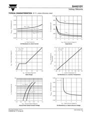
Output Characteristics
0
8
16
24
32
40
012345
V
GS
= 5 thru 2 V
V
DS
- Drain-to-Source Voltage (V)
- Drain Current (A)I
D
1.5 V
Transfer Characteristics
0
8
16
24
32
0.00 0.25 0.50 0.75 1.00 1.25 1.50 1.75
T
C
= 125 °C
- 55 °C
25 °C
V
GS
- Gate-to-Source V oltage (V)
- Drain Current (A) I
D
40
器件 Datasheet 文档搜索
AiEMA 数据库涵盖高达 72,405,303 个元件的数据手册,每天更新 5,000 多个 PDF 文件
