Datasheet 搜索 > 逻辑控制器 > TI(德州仪器) > SN74LVC2G07YZPR 数据手册 > SN74LVC2G07YZPR 数据手册 9/27 页
 器件3D模型
¥ 1.115
SN74LVC2G07YZPR 数据手册 - TI(德州仪器)
制造商:
TI(德州仪器)
分类:
逻辑控制器
封装:
DSBGA-6
描述:
双缓冲/驱动器,具有漏极开路输出 DUAL BUFFER/DRIVER WITH OPEN-DRAIN OUTPUTS
Pictures:
3D模型
符号图
焊盘图
引脚图
产品图
页面导航:
引脚图在P3Hot
典型应用电路图在P9P10
原理图在P1P8
封装尺寸在P12P14P15P24
焊盘布局在P25
标记信息在P12P13
封装信息在P11P12P13P14P15
技术参数、封装参数在P4P9
应用领域在P1P13
电气规格在P5
型号编号列表在P9
导航目录
SN74LVC2G07YZPR数据手册
Page:
of 27 Go
若手册格式错乱,请下载阅览PDF原文件
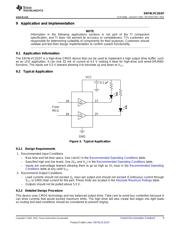
GND
VCC
0.1 F
From
MCU
1A
2A
1Y
2Y
9
SN74LVC2G07
www.ti.com
SCES308L –AUGUST 2001–REVISED MAY 2015
Product Folder Links: SN74LVC2G07
Submit Documentation FeedbackCopyright © 2001–2015, Texas Instruments Incorporated
9 Application and Implementation
NOTE
Information in the following applications sections is not part of the TI component
specification, and TI does not warrant its accuracy or completeness. TI’s customers are
responsible for determining suitability of components for their purposes. Customers should
validate and test their design implementation to confirm system functionality.
9.1 Application Information
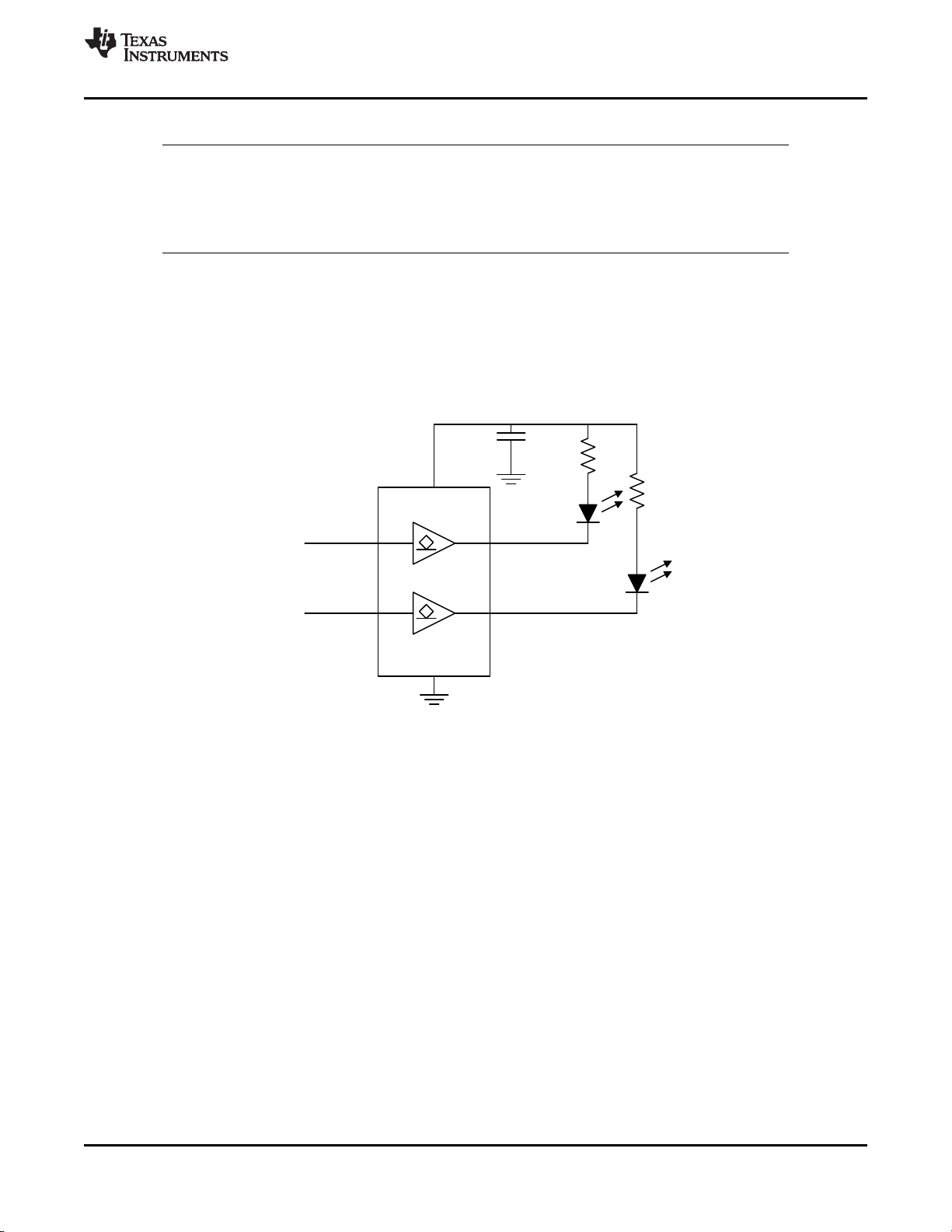
The SN74LVC2G07 is a high-drive CMOS device that can be used to implement a high output drive buffer, such
as an LED application. It can sink 32 mA of current at 4.5 V making it ideal for high-drive and wired-OR/AND
functions. The inputs are 5.5 V tolerant allowing it to translate up and down to V
CC
.
9.2 Typical Application
Figure 3. Typical Application
9.2.1 Design Requirements
1. Recommended Input Conditions
– Rise time and fall time specs. See (Δt/ΔV) in the Recommended Operating Conditions table.
– Specified high and low levels. See (V
IH
and V
IL
) in the Recommended Operating Conditions table.
– Inputs are overvoltage tolerant allowing them to go as high as (V
I
max) in the Recommended Operating
Conditions table at any valid V
CC
.
2. Recommend Output Conditions
– Load currents should not exceed (I
O
max) per output and should not exceed (Continuous current through
V
CC
or GND) total current for the part. These limits are located in the Absolute Maximum Ratings table.
– Outputs should not be pulled above 5.5 V.
9.2.2 Detailed Design Procedure
This device uses CMOS technology and has balanced output drive. Take care to avoid bus contention because it
can drive currents that would exceed maximum limits. The high drive will also create fast edges into light loads
so routing and load conditions should be considered to prevent ringing.
器件 Datasheet 文档搜索
AiEMA 数据库涵盖高达 72,405,303 个元件的数据手册,每天更新 5,000 多个 PDF 文件
