Datasheet 搜索 > Flash芯片 > Winbond Electronics(华邦电子股份) > W25Q64FVSSIG 数据手册 > W25Q64FVSSIG 数据手册 11/92 页
 器件3D模型
¥ 9.537
W25Q64FVSSIG 数据手册 - Winbond Electronics(华邦电子股份)
制造商:
Winbond Electronics(华邦电子股份)
分类:
Flash芯片
封装:
SOIC-8
描述:
64-Mbit(8M x 8bit),SPI接口,工作电压:2.7V to 3.6V
Pictures:
3D模型
符号图
焊盘图
引脚图
产品图
页面导航:
引脚图在P6P7P8P11Hot
原理图在P12
型号编码规则在P89
标记信息在P90
封装信息在P5P89
功能描述在P5P13
技术参数、封装参数在P72
应用领域在P15
电气规格在P30P31P33P34P66P72P74P76P77
型号编号列表在P90
导航目录
W25Q64FVSSIG数据手册
Page:
of 92 Go
若手册格式错乱,请下载阅览PDF原文件

W25Q64FV
Publication Release Date: June 14, 2016
- 11 - Revision Q
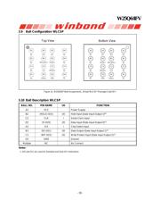
4. PIN DESCRIPTIONS
4.1 Chip Select (/CS)
The SPI Chip Select (/CS) pin enables and disables device operation. When /CS is high, the device is
deselected and the Serial Data Output (DO, or IO0, IO1, IO2, IO3) pins are at high impedance. When
deselected, the devices power consumption will be at standby levels unless an internal erase, program or
write status register cycle is in progress. When /CS is brought low, the device will be selected, power
consumption will increase to active levels and instructions can be written to and data read from the device.
After power-up, /CS must transition from high to low before a new instruction will be accepted. The /CS
input must track the VCC supply level at power-up and power-down (see “Write Protection” and figure 43).
If needed a pull-up resister on /CS can be used to accomplish this.
4.2 Serial Data Input, Output and IOs (DI, DO and IO0, IO1, IO2, IO3)
The W25Q64FV supports standard SPI, Dual SPI, Quad SPI and QPI operation. Standard SPI
instructions use the unidirectional DI (input) pin to serially write instructions, addresses or data to the
device on the rising edge of the Serial Clock (CLK) input pin. Standard SPI also uses the unidirectional DO
(output) to read data or status from the device on the falling edge of CLK.
Dual/Quad SPI and QPI instructions use the bidirectional IO pins to serially write instructions, addresses
or data to the device on the rising edge of CLK and read data or status from the device on the falling edge
of CLK. Quad SPI and QPI instructions require the non-volatile Quad Enable bit (QE) in Status Register-2
to be set. When QE=1, the /WP pin becomes IO2 and /HOLD pin becomes IO3.
4.3 Write Protect (/WP)
The Write Protect (/WP) pin can be used to prevent the Status Registers from being written. Used in
conjunction with the Status Register’s Block Protect (CMP, SEC, TB, BP2, BP1 and BP0) bits and Status
Register Protect (SRP) bits, a portion as small as a 4KB sector or the entire memory array can be
hardware protected. The /WP pin is active low. However, when the QE bit of Status Register-2 is set for
Quad I/O, the /WP pin function is not available since this pin is used for IO2. See figure 1a, 1b and 1c for
the pin configuration of Quad I/O operation.
4.4 HOLD (/HOLD)
The /HOLD pin allows the device to be paused while it is actively selected. When /HOLD is brought low,
while /CS is low, the DO pin will be at high impedance and signals on the DI and CLK pins will be ignored
(don’t care). When /HOLD is brought high, device operation can resume. The /HOLD function can be
useful when multiple devices are sharing the same SPI signals. The /HOLD pin is active low. When the
QE bit of Status Register-2 is set for Quad I/O, the /HOLD pin function is not available since this pin is
used for IO3. See figure 1a, 1b and 1c for the pin configuration of Quad I/O operation.
4.5 Serial Clock (CLK)
The SPI Serial Clock Input (CLK) pin provides the timing for serial input and output operations. ("See SPI
Operations")
器件 Datasheet 文档搜索
AiEMA 数据库涵盖高达 72,405,303 个元件的数据手册,每天更新 5,000 多个 PDF 文件
