Datasheet 搜索 > TVS二极管 > Microsemi(美高森美) > JANTXV1N5811US 数据手册 > JANTXV1N5811US 其他数据使用手册 2/3 页


¥ 102.675
JANTXV1N5811US 其他数据使用手册 - Microsemi(美高森美)
制造商:
Microsemi(美高森美)
分类:
TVS二极管
封装:
E-MELF
Pictures:
3D模型
符号图
焊盘图
引脚图
产品图
页面导航:
应用领域在P1P3
导航目录
JANTXV1N5811US数据手册
Page:
of 3 Go
若手册格式错乱,请下载阅览PDF原文件
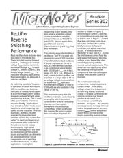
Only after this peak occurs will
reverse current diminish in the
latter portion of switching. The
overall time these semiconductor
events occur to switch off current
flow in the rectifier is represented
by reverse recovery time t
rr
.
In lower current applications, the
reverse current overshoot for
charge recovery is often limited by
the circuit or test method used
rather than the diode itself. When
test limited in this manner, it is then
simply identified as reverse
current I
RM
as shown in Figure 2.
This is an important distinction
from I
RM(REC)
since I
RM
is not a
diode dependent feature.
In either case, recovered charge
Q
RR
may be approximated by area
under the reverse current-time
curve. This Q
RR
also represents
energy that must be dissipated with
reverse voltage in the power
switching side of the circuit. In
Figure 1 where it appears
triangular and the apex is at
I
RM(REC)
, recovered charge Q
RR
can
be approximated by the
expression:
Q
RR
∼ (1/2) t
rr
I
RM(REC)
When I
RM
is limited by application
or test circuit, it will extend t
rr
somewhat to recover the charge
Q
RR
. It is also apparent that high
forward operating currents (I
O
)
injecting greater stored charge will
Series 302
require longer reverse recovery
time to switch. If I
O
and V
F
conduction losses result in higher
operating temperature, this will
also effectively increase t
rr
,
I
RM(REC)
, and
switching losses.
Both suggest rectifiers should be
conservatively chosen in I
O
ratings
versus application including any
noted I
F
difference in t
rr
test
characterization.
The reverse recovery time t
rr
is
comprised of two time intervals t
a
and t
b
when rectifiers respond with
their own peak reverse recovery
current I
RM(REC)
as shown in Figure
1. The t
a
begins at the moment
forward current has been ramped
down from I
F
where it intersects
the zero current axis, and
concludes at
the rectifier I
RM(REC)
peak response
point.
This t
a
region is primarily dictated
by rectifier component design in
how quickly the I
RM(REC)
peak can
be achieved with minority carrier
lifetime control. During this t
a
portion of switching, other circuit
components may be subjected to
fast rise time voltage-current
where the rectifier has not yet
begun to support reverse voltage.
As switching rates (di/dt)
increase, these other components
must absorb corresponding
greater switching energy and
heating. As operating frequency
increases, this can be excessive
at high duty factors.
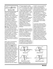
The latter part of reverse recovery
time is t
b
. It begins at I
RM(REC)
peak and ends where reverse
current
decays to a specified level (see
Figure 1). In low to medium current
“soft recovery” rectifiers, it is often
where i
R
diminishes to 10-
25% of the specified peak I
RM
test
value. On higher rated current
rectifiers, reverse recovery may
also be specified to end at an
intercept point on the zero-current
axis after drawing a straight line
from the I
RM(REC)
point to 0.25
I
RM(REC)
on the recovery curve. This
line is then extended to the
termination point on the zero-axis.
For rectifiers with “abrupt recovery”
or oscillatory ring-off, it is where
reverse current again crosses the
zero axis. These examples are in
Figure 3.
The t
b
region in reverse recovery is
influenced by rectifier design and
circuit interaction. It is this
switching region where the rectifier
is now supporting significant
reverse voltage while reverse
current is still diminishing. During
this brief time, voltage and reverse
current switching energy are now
primarily absorbed by the rectifier.
This can also generate notable
rectifier heating if t
b
is excessively
long, particularly if repeated at
high frequency.
From the combined effects of both
t
a
and t
b
for reverse recovery time,
it is apparent that minimal values of
t
rr
are needed to reduce switching
energy stresses to other
components as well as the rectifier
diode itself in higher speed
applications. Since t
b
(and I
RM
)
are also influenced by the circuit, it
is important to specify test
requirements for t
rr
that reasonably
approximate actual operating
conditions including forward
current, di/dt, and temperature.
The latest industry standards for
measuring reverse recovery time
are found in JEDEC Standard
JESD41 which is virtually identical
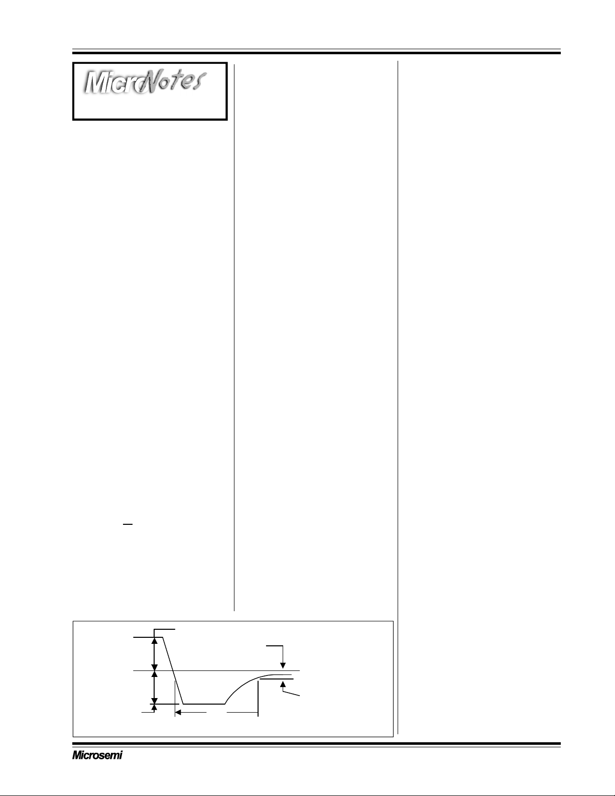
Figure 2. Circuit Limited I
RM
0.10 I
RM
or 0.25 I
RM
I
R(REC)
I
F
t
rr
器件 Datasheet 文档搜索
AiEMA 数据库涵盖高达 72,405,303 个元件的数据手册,每天更新 5,000 多个 PDF 文件
