Datasheet 搜索 > 编解码器 > ADI(亚德诺) > AD1938WBSTZ 数据手册 > AD1938WBSTZ 产品设计参考手册 5/32 页
 器件3D模型
¥ 22.788
AD1938WBSTZ 产品设计参考手册 - ADI(亚德诺)
制造商:
ADI(亚德诺)
分类:
编解码器
封装:
LQFP-48
描述:
ANALOG DEVICES AD1938WBSTZ 音频编解码器, AEC-Q100, 立体声, 4, 8, -40 °C, 105 °C, 192 kSPS
Pictures:
3D模型
符号图
焊盘图
引脚图
产品图
页面导航:
原理图在P9P10P11P12P13P14P15P16P17
型号编码规则在P26

导航目录
AD1938WBSTZ数据手册
Page:
of 32 Go
若手册格式错乱,请下载阅览PDF原文件
Evaluation Board User Guide UG-045
Rev. 0 | Page 5 of 32
08421-011
JP31
HDR1
JP30
HDR2
JP29
8416
JP28
CLK
JP24
OSC
R155
R156
C154
C153
MCLKI
XTAL
MCLKO
XTAL
R166
R178
MCLKI BUS
MCLKO BUS
JP27
HDR1
JP25
HDR2
JP23
CPLD
OSC DISABLE
193X_MCLKI
DISABLE
EXT
EXT CLK IN
193X_MCLKO
1938_MCLKI
R160
R167
R169
R172
R174
R175
C168
C170
JP22
C158
L7
JP19
JP18
JP20
C147
U21
U18
U22
Y1
J23
J22
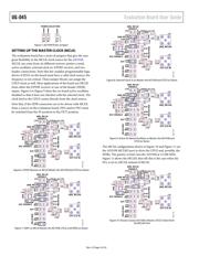
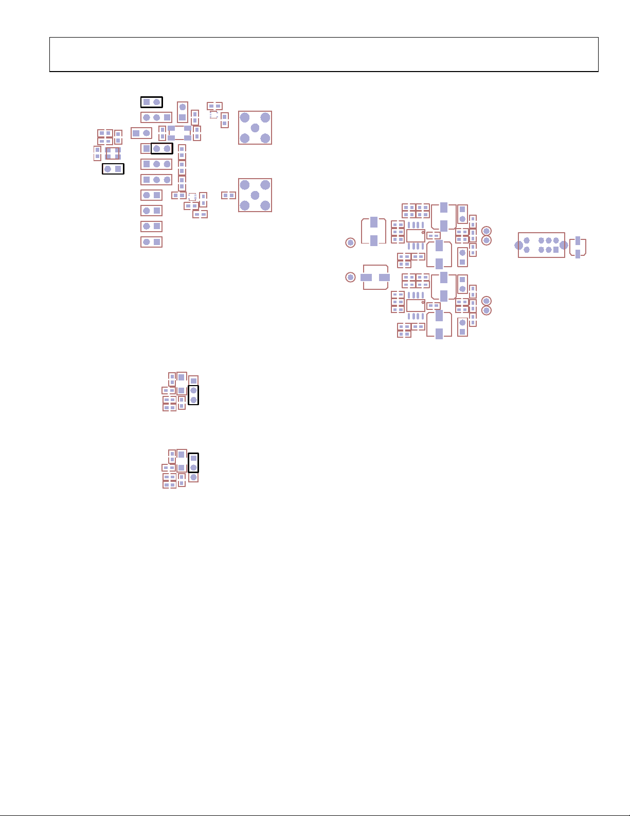
Figure 11. LRCLK Is the Master Clock Using the PLL; MCLKI Is Disabled, and
CPLD Is Slave to the MCLKO Port
CONFIGURING THE PLL FILTER
The PLL for the AD1938 can run from either MCLK or LRCLK,
according to its setting in the PLL and Clock Control 0 register,
Bits[6:5]. The matching RC loop filter must be connected to LF
(Pin 47) using JP15. See Figure 12 and Figure 13 for the jumper
positions.
08421-012
C114
C120
C131
JP15
MCLK LRCLK
R129
C125
R138
PLL SELECT
Figure 12. MCLK Loop Filter Selected
08421-013
C114
C120
C131
JP15
MCLK LRCLK
R129
C125
R138
PLL SELECT
Figure 13. LRCLK Loop Filter Selected
Normally, the MCLK filter is the default selection; it is also
possible to use the register control window to program the
PLL to run from the LRCLK. In this case, the jumper must
be changed as shown in Figure 13.
CONNECTING AUDIO CABLES
Analog Audio
The analog inputs and outputs use 3.5 mm TRS jacks; they are
configured in the standard configuration: tip = left, ring = right,
sleeve = ground. The analog inputs to IN1 and IN2 generate
0 dBFS from a 1 V rms analog signal. The on-board buffer circuit
creates the differential signal to drive the ADC with 2 V rms at
the maximum level. The DAC puts out a 0.8775 V rms single-
ended signal at 0 dBFS; this signal is buffered and filtered before
the OUT connectors. There are test points that allow direct
access to the ADC and DAC pins; note that the ADC and DAC
have a common-mode voltage of 1.5 V dc. These test points
require proper care so that improper loading does not drag
down the common-mode voltage, and the headroom and
performance of the part do not suffer.
The ADC buffer circuit is designed with a switch (S1) that
allows the user to change the voltage reference for all of the
amplifiers. GND, CM, and FILTR can be selected as a reference;
it is advisable to shut down the power to the board before
changing this switch. The CM and FILTR lines are very
sensitive and do not react well to a change in load while the
AD1938 is active. A series of jumpers allows the user to dc-
couple the buffer circuit to the ADC analog port when CM and
FILTR are selected (see Figure 14).
08421-014
R72
C60
R73
S1 C74
C63
C61
C64
C65
C67
C69
R84
R86
C76
C99
R106
R107
U14
C77
C82
C80
C83
C88
R85
R87
TP32
TP28
VREF SELECT
TP26
IN1R+
IN1R–
IN1L+
IN1L–
TP34
R79R77C62
C66
C79R97
R93
JP12
R90
C89
R76
GND
FILTER
CM
JP4
C68
C72
JP11
R81
R101
JP13
C105
C75
U12
TP25
IN1L
IN1R
TP30
Figure 14. VREF Selection and DC Coupling Jumpers
Digital Audio
There are two types of digital interfacing, S/PDIF and discrete
serial. The input and output S/PDIF ports have optical and
coaxial connectors. The serial audio connectors use 1 × 2 100 mil
spaced headers with pins for both signal and ground. The
LRCLK, BCLK, and SDATA paths are available for both the
ADC and DAC on the HDR1 and HDR2 connectors. Each has a
connection for MCLK; each HDR MCLK interface has a switch
to set the port as an input or output, depending on the master
or slave state of the AD1938.
SWITCH AND JUMPER SETTINGS
Clock and Control
The AD1938 is designed to run in standalone mode at a sample
rate (f
S
) of 48 kHz, with an MCLK of 12.288 MHz (256 × f
S
). In
standalone slave mode, both ADC and DAC ports must receive
valid BCLK and LRCLK. The AD1938 can be clocked from
either the S/PDIF receiver or the HDR1 connector; the ADC
BCLK and LRCK port sources are selected with S2, Position 2
and Position 3. For the S/PDIF master, both switches should be
off. For HDR1, S2, Position 3, should be on (see the detail in
Figure 15 and Figure 16). The DAC BCLK and LRCK port
sources are selected with S2, Position 5 and Position 6. For the
S/PDIF master, both switches should be off. For HDR1, S2,
Position 6, should be on. Note that HDR2 is not implemented
in the CPLD routing code.
It is also possible to configure the AD1938 ADC BCLK and
LRCK ports to run in standalone master mode; moving J5 to
SDA/1, as shown in Figure 3, changes the state of the AD1938.
Setting S2, Position 2 and Position 5, to on selects the proper
routing to both the S/PDIF receiver and the HDR1 connector.
器件 Datasheet 文档搜索
AiEMA 数据库涵盖高达 72,405,303 个元件的数据手册,每天更新 5,000 多个 PDF 文件
