Datasheet 搜索 > DA转换器 > ADI(亚德诺) > AD5331BRU-REEL7 数据手册 > AD5331BRU-REEL7 数据手册 2/28 页


¥ 0
AD5331BRU-REEL7 数据手册 - ADI(亚德诺)
制造商:
ADI(亚德诺)
分类:
DA转换器
封装:
TSSOP
描述:
2.5 V至5.5 V , 115 μA ,并行接口单电压输出8位/ 10位/ 12位DAC 2.5 V to 5.5 V, 115 μA, Parallel Interface Single Voltage-Output 8-/10-/12-Bit DACs
Pictures:
3D模型
符号图
焊盘图
引脚图
产品图
页面导航:
引脚图在P7P8P9P10P23Hot
典型应用电路图在P21
原理图在P1P7P8P9P10
封装尺寸在P24
型号编码规则在P25
焊接温度在P6
功能描述在P1P7P8P9P10
技术参数、封装参数在P1P3P6
应用领域在P1P21
电气规格在P13
导航目录
AD5331BRU-REEL7数据手册
Page:
of 28 Go
若手册格式错乱,请下载阅览PDF原文件

AD5330/AD5331/AD5340/AD5341
Rev. A | Page 2 of 28
TABLE OF CONTENTS
Features .............................................................................................. 1
Applications ....................................................................................... 1
General Description ......................................................................... 1
Functional Block Diagram .............................................................. 1
Revision History ............................................................................... 2
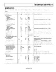
Specifications ..................................................................................... 3
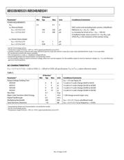
AC Characteristics ........................................................................ 4
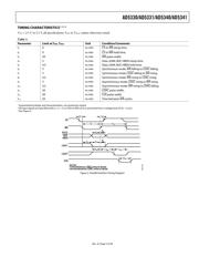
Timing Characteristics ................................................................ 5
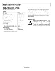
Absolute Maximum Ratings ............................................................ 6
ESD Caution .................................................................................. 6
Pin Configurations and Function Descriptions ........................... 7
Terminology .................................................................................... 11
Typical Performance Characteristics ........................................... 13
Theory of Operation ...................................................................... 17
Digital-to-Analog Section ......................................................... 17
Resistor String ............................................................................. 17
DAC Reference Input ................................................................. 17
Output Amplifier ........................................................................ 17
Parallel Interface ............................................................................. 18
Double-Buffered Interface ........................................................ 18
Clear Input (
CLR
) ...................................................................... 18
Chip Select Input (
CS
) ............................................................... 18
Write Input (
WR
) ....................................................................... 18
Load DAC Input (
LDAC
) .......................................................... 18
High-Byte Enable Input (HBEN) ............................................. 18
Power-On Reset .......................................................................... 18
Power-Down Mode ........................................................................ 19
Suggested Databus Formats .......................................................... 20
Applications Information .............................................................. 21
Typical Application Circuits ..................................................... 21
Driving V
DD
From the Reference Voltage ............................... 21
Bipolar Operation Using the AD5330/AD5331/
AD5340/AD5341 ......................................................................... 21
Decoding Multiple AD5330/AD5331/ AD5340/AD5341 .... 21
Programmable Current Source ................................................ 22
Power Supply Bypassing and Grounding ................................ 22
Outline Dimensions ....................................................................... 24
Ordering Guide .......................................................................... 25
REVISION HISTORY
2/08—Rev. 0 to Rev. A
Updated Format .................................................................. Universal
Changes to Table 4 .......................................................................... 16
Replaced Driving V
DD
from the Reference Voltage Section ..... 21
Updated Outline Dimensions ....................................................... 24
Changes to Ordering Guide .......................................................... 25
4/00—Revision 0: Initial Version
器件 Datasheet 文档搜索
AiEMA 数据库涵盖高达 72,405,303 个元件的数据手册,每天更新 5,000 多个 PDF 文件
