Datasheet 搜索 > DA转换器 > ADI(亚德诺) > AD5331BRU-REEL7 数据手册 > AD5331BRU-REEL7 数据手册 3/28 页


¥ 0
AD5331BRU-REEL7 数据手册 - ADI(亚德诺)
制造商:
ADI(亚德诺)
分类:
DA转换器
封装:
TSSOP
描述:
2.5 V至5.5 V , 115 μA ,并行接口单电压输出8位/ 10位/ 12位DAC 2.5 V to 5.5 V, 115 μA, Parallel Interface Single Voltage-Output 8-/10-/12-Bit DACs
Pictures:
3D模型
符号图
焊盘图
引脚图
产品图
页面导航:
引脚图在P7P8P9P10P23Hot
典型应用电路图在P21
原理图在P1P7P8P9P10
封装尺寸在P24
型号编码规则在P25
焊接温度在P6
功能描述在P1P7P8P9P10
技术参数、封装参数在P1P3P6
应用领域在P1P21
电气规格在P13
导航目录
AD5331BRU-REEL7数据手册
Page:
of 28 Go
若手册格式错乱,请下载阅览PDF原文件

AD5330/AD5331/AD5340/AD5341
Rev. A | Page 3 of 28
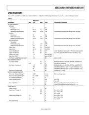
SPECIFICATIONS
V
DD
= 2.5 V to 5.5 V, V
REF
= 2 V, R
L
= 2 kΩ to GND; C
L
= 200 pF to GND; all specifications T
MIN
to T
MAX
, unless otherwise noted.
Table 1.
Parameter
1
B Version
2
Unit Conditions/Comments Min Typ Max
DC PERFORMANCE
3, 4
AD5330
Resolution 8 Bits
Relative Accuracy ±0.15 ±1 LSB
Differential Nonlinearity ±0.02 ±0.25 LSB Guaranteed monotonic by design over all codes
AD5331
Resolution 10 Bits
Relative Accuracy ±0.5 ±4 LSB
Differential Nonlinearity ±0.05 ±0.5 LSB Guaranteed monotonic by design over all codes
AD5340/AD5341
Resolution 12 Bits
Relative Accuracy ±2 ±16 LSBs
Differential Nonlinearity ±0.2 ±1 LSB Guaranteed monotonic by design over all codes
Offset Error ±0.4 ±3 % of FSR
Gain Error ±0.15 ±1 % of FSR
Lower Deadband
5
10 60 mV Lower deadband exists only if offset error is negative
Upper Deadband 10 60 mV V
DD
= 5 V; upper deadband exists only if V
REF
= V
DD
Offset Error Drift
6
−12 ppm of FSR/°C
Gain Error Drift
6
−5 ppm of FSR/°C
DC Power Supply Rejection Ratio
6
−60 dB ΔV
DD
= ±10%
DAC REFERENCE INPUT
6
V
REF
Input Range 1 V
DD
V Buffered reference (AD5330, AD5340, and AD5341)
0.25 V
DD
V Unbuffered reference
V
REF
Input Impedance >10 MΩ Buffered reference (AD5330, AD5340, and AD5341)
180 kΩ Unbuffered reference; gain = 1, input impedance = R
DAC
90 kΩ Unbuffered reference; gain = 2, input impedance = R
DAC
Reference Feedthrough −90 dB Frequency = 10 kHz
OUTPUT CHARACTERISTICS
6
Minimum Output Voltage
4, 7
0.001 V min Rail-to-rail operation
Maximum Output Voltage
4, 7
V
DD
− 0.001 V max
DC Output Impedance 0.5 Ω
Short-Circuit Current 25 mA V
DD
= 5 V
15 mA V
DD
= 3 V
Power-Up Time 2.5 μs Coming out of power-down mode; V
DD
= 5 V
5 μs Coming out of power-down mode; V
DD
= 3 V
LOGIC INPUTS
6
Input Current ±1 μA
Input Low Voltage, V
IL
0.8 V V
DD
= 5 V ± 10%
0.6 V V
DD
= 3 V ± 10%
0.5 V V
DD
= 2.5 V
Input High Voltage, V
IH
2.4 V V
DD
= 5 V ± 10%
2.1 V V
DD
= 3 V ± 10%
2.0 V V
DD
= 2.5 V
Pin Capacitance 3 pF
器件 Datasheet 文档搜索
AiEMA 数据库涵盖高达 72,405,303 个元件的数据手册,每天更新 5,000 多个 PDF 文件
