Datasheet 搜索 > DSP数字信号处理器 > ADI(亚德诺) > ADSP-BF514BBCZ-3 数据手册 > ADSP-BF514BBCZ-3 数据手册 4/68 页
 器件3D模型
¥ 7.264
ADSP-BF514BBCZ-3 数据手册 - ADI(亚德诺)
制造商:
ADI(亚德诺)
分类:
DSP数字信号处理器
封装:
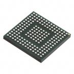
LFBGA-168
描述:
Blackfin嵌入式处理器 Blackfin Embedded Processor
Pictures:
3D模型
符号图
焊盘图
引脚图
产品图
页面导航:
引脚图在P59P60Hot
原理图在P1P6
封装尺寸在P28P65
型号编码规则在P23P28P67
功能描述在P3P12
技术参数、封装参数在P1P9P13P22P27P29P55P67
应用领域在P1
电气规格在P24P25P26P27
导航目录
ADSP-BF514BBCZ-3数据手册
Page:
of 68 Go
若手册格式错乱,请下载阅览PDF原文件
Rev. D | Page 4 of 68 | April 2014
ADSP-BF512/BF514/BF514F16/BF516/BF518/BF518F16
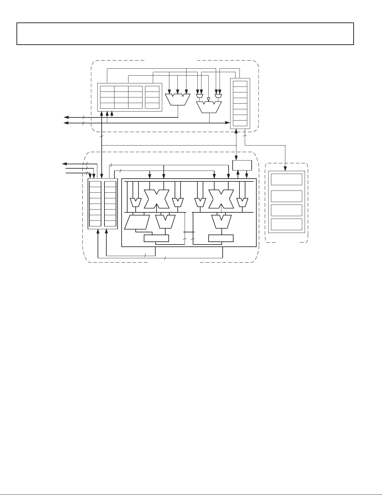
For certain instructions, two 16-bit ALU operations can be per-
formed simultaneously on register pairs (a 16-bit high half and
16-bit low half of a compute register). If the second ALU is used,
quad 16-bit operations are possible.
The 40-bit shifter can perform shifts and rotates and is used to
support normalization, field extract, and field deposit
instructions.
The program sequencer controls the flow of instruction execu-
tion, including instruction alignment and decoding. For
program flow control, the sequencer supports PC relative and
indirect conditional jumps (with static branch prediction), and
subroutine calls. Hardware is provided to support zero-over-
head looping. The architecture is fully interlocked, meaning that
the programmer need not manage the pipeline when executing
instructions with data dependencies.
The address arithmetic unit provides two addresses for simulta-
neous dual fetches from memory. It contains a multiported
register file consisting of four sets of 32-bit index, modify,
length, and base registers (for circular buffering), and eight
additional 32-bit pointer registers (for C-style indexed stack
manipulation).
Blackfin processors support a modified Harvard architecture in
combination with a hierarchical memory structure. Level 1 (L1)
memories are those that typically operate at the full processor
speed with little or no latency. At the L1 level, the instruction
memory holds instructions only. The two data memories hold
data, and a dedicated scratchpad data memory stores stack and
local variable information.
In addition, multiple L1 memory blocks are provided, offering a
configurable mix of SRAM and cache. The memory manage-
ment unit (MMU) provides memory protection for individual
tasks that may be operating on the core and can protect system
registers from unintended access.
The architecture provides three modes of operation: user mode,
supervisor mode, and emulation mode. User mode has
restricted access to certain system resources, thus providing a
protected software environment, while supervisor mode has
unrestricted access to the system and core resources.
The Blackfin processor instruction set has been optimized so
that 16-bit opcodes represent the most frequently used instruc-
tions, resulting in excellent compiled code density. Complex
DSP instructions are encoded into 32-bit opcodes, representing
fully featured multifunction instructions. Blackfin processors
support a limited multi-issue capability, where a 32-bit
Figure 2. Blackfin Processor Core
SEQUENCER
ALIGN
DECODE
LOOP BUFFER
16
16
8888
40 40
A0 A1
BARREL
SHIFTER
DATA ARITHMETIC UNIT
CONTROL
UNIT
R7.H
R6.H
R5.H
R4.H
R3.H
R2.H
R1.H
R0.H
R7.L
R6.L
R5.L
R4.L
R3.L
R2.L
R1.L
R0.L
ASTAT
40 40
32
32
32
32
32
32
32LD0
LD1
SD
DAG0
DAG1
ADDRESS ARITHMETIC UNIT
I3
I2
I1
I0
L3
L2
L1
L0
B3
B2
B1
B0
M3
M2
M1
M0
SP
FP
P5
P4
P3
P2
P1
P0
DA1
DA0
32
32
32
PREG
RAB
32
TO MEMORY
器件 Datasheet 文档搜索
AiEMA 数据库涵盖高达 72,405,303 个元件的数据手册,每天更新 5,000 多个 PDF 文件
