Datasheet 搜索 > DSP数字信号处理器 > ADI(亚德诺) > ADSP-BF514BBCZ-3 数据手册 > ADSP-BF514BBCZ-3 数据手册 6/68 页
 器件3D模型
¥ 7.264
ADSP-BF514BBCZ-3 数据手册 - ADI(亚德诺)
制造商:
ADI(亚德诺)
分类:
DSP数字信号处理器
封装:
LFBGA-168
描述:
Blackfin嵌入式处理器 Blackfin Embedded Processor
Pictures:
3D模型
符号图
焊盘图
引脚图
产品图
页面导航:
引脚图在P59P60Hot
原理图在P1P6
封装尺寸在P28P65
型号编码规则在P23P28P67
功能描述在P3P12
技术参数、封装参数在P1P9P13P22P27P29P55P67
应用领域在P1
电气规格在P24P25P26P27
导航目录
ADSP-BF514BBCZ-3数据手册
Page:
of 68 Go
若手册格式错乱,请下载阅览PDF原文件
Rev. D | Page 6 of 68 | April 2014
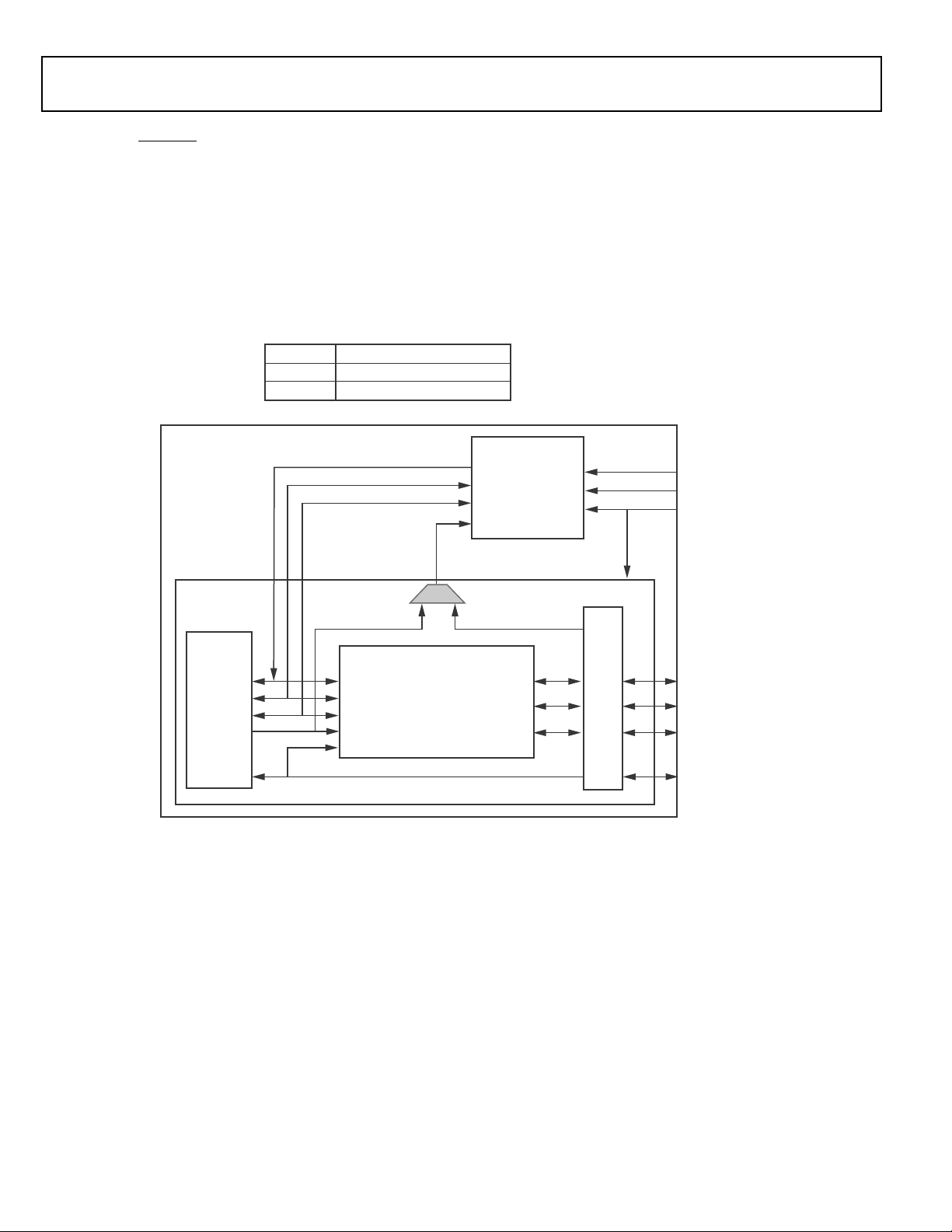
ADSP-BF512/BF514/BF514F16/BF516/BF518/BF518F16
The processors internally connect to the flash memory die with
the SPI0SCK, SPI0SEL4
or PH8, SPI0MOSI, and SPI0MISO sig-
nals similar to an external SPI flash (for signal descriptions, see
Table 2). To further provide a secure processing environment,
these internally connected signals are not exposed outside of the
package. For this reason, programming the ADSP-BF51xF flash
memory is performed by running code on the processor and
cannot be programmed from external signals. Data transfers
between the SPI flash and the processor cannot be probed exter-
nally. The flash memory has the following additional features.
• Serial Interface Architecture—SPI compatible with Mode 0
and Mode 3
• Flexible Erase Capability—Uniform 4K Byte sectors and
uniform 64K Byte overlay blocks
• Fast Erase and Byte-Program—Chip-erase time = 11.2 s
(typical), Sector-/Block-Erase Time = 70/350 ms (typical)
Byte-Program Time = 15 μS (typical)
• Software Write Protection—Write protection through
block-protection bits in status register
Figure 4. Flash Memory Block Diagram
MISO_EXT
SPICLK_EXT
SEL4
Combinational Logic
SPICLK_INT
MOSI_INT
SPISS
MOSI_EXT
MISO_INT
SEL4
SPICLK
MOSI
MISO
M
U
X
L
O
G
I
C
SPISS
VDD
GND
RST
SPI Flash Die
SO
SCK
CE
SI
VDDFLASH
GND
RESET
PG13
-
SPI0MISO
PG12
-
SPI0SCK
PG14
-
SPI0MOSI
PG11
-
SPI0SS
SEL4
PH8
RESET
SEL4 or PH8
MISO_EXT, SPICLK_EXT, MOSI_EXT
0
1
Three-state
As programmed
Combinational Logic
Truth Table
ADSP-BF51xF
Package
Signals between the processor and the flash
operate at the VDDFLASH voltage level.
SPI0 signals external
to the processor
operate at the
VDDEXT voltage
level.
SPI0
ADSP-BF51x Die
器件 Datasheet 文档搜索
AiEMA 数据库涵盖高达 72,405,303 个元件的数据手册,每天更新 5,000 多个 PDF 文件
