Datasheet 搜索 > DSP数字信号处理器 > ADI(亚德诺) > ADSP-BF514BBCZ-3 数据手册 > ADSP-BF514BBCZ-3 数据手册 5/68 页
 器件3D模型
¥ 7.264
ADSP-BF514BBCZ-3 数据手册 - ADI(亚德诺)
制造商:
ADI(亚德诺)
分类:
DSP数字信号处理器
封装:
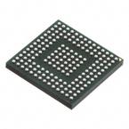
LFBGA-168
描述:
Blackfin嵌入式处理器 Blackfin Embedded Processor
Pictures:
3D模型
符号图
焊盘图
引脚图
产品图
页面导航:
引脚图在P59P60Hot
原理图在P1P6
封装尺寸在P28P65
型号编码规则在P23P28P67
功能描述在P3P12
技术参数、封装参数在P1P9P13P22P27P29P55P67
应用领域在P1
电气规格在P24P25P26P27
导航目录
ADSP-BF514BBCZ-3数据手册
Page:
of 68 Go
若手册格式错乱,请下载阅览PDF原文件
ADSP-BF512/BF514/BF514F16/BF516/BF518/BF518F16
Rev. D | Page 5 of 68 | April 2014
instruction can be issued in parallel with two 16-bit instruc-
tions, allowing the programmer to use many of the core
resources in a single instruction cycle.
The Blackfin processor assembly language uses an algebraic syn-
tax for ease of coding and readability. The architecture has been
optimized for use in conjunction with the C/C++ compiler,
resulting in fast and efficient software implementations.
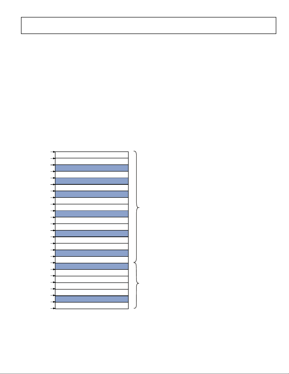
MEMORY ARCHITECTURE
The ADSP-BF51x processors view memory as a single unified
4G byte address space, using 32-bit addresses. All resources,
including internal memory, external memory, and I/O control
registers, occupy separate sections of this common address
space. The memory portions of this address space are arranged
in a hierarchical structure to provide a good cost/performance
balance of some very fast, low-latency on-chip memory as cache
or SRAM, and larger, lower-cost and performance off-chip
memory systems. The memory map for both internal and exter-
nal memory space is shown in Figure 3.
The on-chip L1 memory system is the highest-performance
memory available to the Blackfin processor. The off-chip mem-
ory system, accessed through the external bus interface unit
(EBIU), provides expansion with SDRAM, flash memory, and
SRAM, optionally accessing up to 132M bytes of
physical memory.
The memory DMA controller provides high bandwidth data-
movement capability. It can perform block transfers of code or
data between the internal memory and the external
memory spaces.
Internal (On-Chip) Memory
The ADSP-BF51x processors have three blocks of on-chip
memory that provide high bandwidth access to the core.
The first block is the L1 instruction memory, consisting of
48K bytes SRAM, of which 16K bytes can be configured as a
four-way set-associative cache. This memory is accessed at full
processor speed.
The second on-chip memory block is the L1 data memory, con-
sisting of up to two banks of up to 32K bytes each. Each memory
bank is configurable, offering both cache and SRAM functional-
ity. This memory block is accessed at full processor speed.
The third memory block is a 4K byte scratchpad SRAM which
runs at the same speed as the L1 memories, but is only accessible
as data SRAM and cannot be configured as cache memory.
External (Off-Chip) Memory
External memory is accessed via the EBIU. This 16-bit interface
provides a glueless connection to a bank of synchronous DRAM
(SDRAM) as well as up to four banks of asynchronous memory
devices including flash, EPROM, ROM, SRAM, and memory
mapped I/O devices.
The SDRAM controller can be programmed to interface to up
to 128M bytes of SDRAM. A separate row can be open for each
SDRAM internal bank, and the SDRAM controller supports up
to four internal SDRAM banks, improving overall performance.
The asynchronous memory controller can be programmed to
control up to four banks of devices with very flexible timing
parameters for a wide variety of devices. Each bank occupies a
1M byte segment regardless of the size of the devices used, so
that these banks are only contiguous if each is fully populated
with 1M byte of memory.
Flash Memory
The ADSP-BF51xF processors contain an SPI flash memory
within the package of the processor connected to SPI0
(Figure 4).
The SPI flash memory has a 16M bit capacity. Also included are
support for software write protection and for fast erase and
byte-program.
Figure 3. ADSP-BF51x Internal/External Memory Map
RESERVED
CORE MMR REGISTERS (2M BYTES)
RESERVED
SCRATCHPAD SRAM (4K BYTES)
INSTRUCTION BANK B SRAM (16K BYTES)
SYSTEM MMR REGISTERS (2M BYTES)
RESERVED
RESERVED
DATA BANK B SRAM / CACHE (16K BYTES)
DATA BANK B SRAM (16K BYTES)
DATA BANK A SRAM / CACHE (16K BYTES)
ASYNCMEMORYBANK3(1MBYTES)
ASYNCMEMORYBANK2(1MBYTES)
ASYNCMEMORYBANK1(1MBYTES)
ASYNCMEMORYBANK0(1MBYTES)
INSTRUCTION BANK C SRAM/CACHE (16K BYTES)
IN
T
ER
N
A
L
M
E
MO
R
Y
M
A
P
E
X
T
E
R
NA
L
M
E
M
O
R
Y
M
A
P
0xFFFF FFFF
0x
FFE0 0000
0xFFB0 0000
0xFFA1 4000
0xFFA1 0000
0xFF90 8000
0xFF90 4000
0xFF80 8000
0xFF80 4000
0x2040 0000
0x2030 0000
0x2020 0000
0x2010 0000
0x2000 0000
0xEF00 0000
0x0000 0000
0xFFC0 0000
0xFFB0 1000
0xFFA0 0000
DATA BANK A SRAM (16K BYTES)
0xFF90 0000
0xFF80 0000
RESERVED
RESERVED
0xFFA0 8000
INSTRUCTION BANK A SRAM (16K BYTES)
RESERVED
BOOT ROM (32K BYTES)
0xEF00 8000
RESERVED
0x08 00 0000
0xFFA0 4000
SDRAM MEMORY (16M BYTES
-
128M BYTES)
器件 Datasheet 文档搜索
AiEMA 数据库涵盖高达 72,405,303 个元件的数据手册,每天更新 5,000 多个 PDF 文件
